


Page 4 of 9
V1642OM.DOC
17 February, 2005
2.3 INSERTION
DELAY
SDI to SDI
1.188
µ
s
32 clocks
Parallel processing
0.925
µ
s
25 clocks
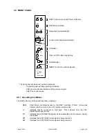
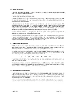
2.4 HARDWARE
The figure below shows diagrammatically the printed circuit board along with certain other components
of interest. In particular it shows the position and orientation of the links and switches which set up the
operation modes.
The EPROM location is shown, as it is the component that would need to be changed as a result of any
software upgrade in the field.
S9
Front Panel
Rear Connector
S1
EPROM
LK4
S6
0
7
0
3
0
7
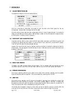
The purposes of the links and switches is shown in the following table. Details of their operation are
described in later sections.
ITEM Title
Section
Comments
S1, 0 to 5
RS485 Address
3.7
Unique address required for all units on the
bus.
S1, 6 & 7
Engineering
Normally both set to ON
S6
RESET
Push to reset the micro-controller
LK 4, 0
625 mode
3.2
De-Hanover bar or Hue shift
LK 4, 1
525 mode
3.2
Hue shift or De-Hanover bar
LK 4, 2
Hard Clip
3.5
LK 4, 3
Disable DR
3.4
LK 4, 4 to 7
reserved
EPROM
The operating programme. Only needs to be
changed for software upgrade.
S9, 0 to 3
RS232/485
3.7
All OFF for RS232. All ON for RS485.


