


Handling with VIPA data handling blocks
Manual BG41/BG42/BG43
4-22
Rev. 99/49
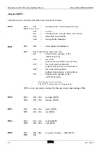
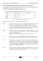
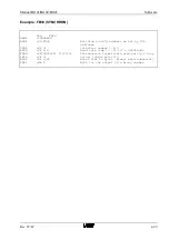
4.1.7.3 FB37 (SYNCHRON) from firmware 401xV50 and all of 4118 for 3964(R)
This data handling block prepares the interface building block for the operation of the procedure
3964(R).
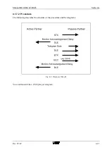
The data handling block must be loaded in all start branches (OB20,21,22) for each interface
channel to be used. If 2 channels are used with the procedure 3964(R), this data handling block
must be loaded twice.
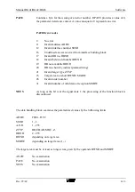
The data handling block has formal operands. Several operating parameters are to be set through
these formal operands. They are only directly addressable.
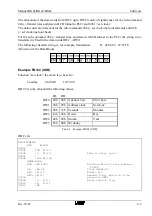
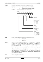
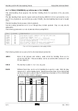
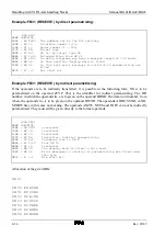
The following parameters are to be transmitted when loading FB37:
Des.
Format
Explanation
ADRE
KH
Address set with the DIL switches
SSNR
KF
Interface number 1,2,3
BAUD
KF
Baud rate code 1...11 (10 = 9600Baud)
FORM
KM
Transmission format:8bit,even parity,2 stop
PRIO
KF
0=low, 1=high priority
BLOC
KF
Block size in bytes (always even-numbered!)
ZVZ
KF
Character delay time (value*10ms)
QVZ
KF
Acknowledgement delay time (value*10ms)
PAFE
MB
Byte for the output of a wrong number
NEUS
M
Blocks the building block
Tab. 4-10:List of parameters for the loading of FB37
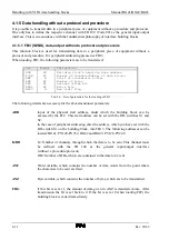
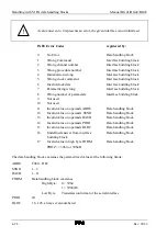
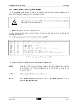
The following details are necessary for the abovementioned parameters:
ADRE
Input of the physical start address, under which the building block can be
accessed by the PLC. This start address can be set with the DIL switches S1 and
S2 (see chapter 5).
SSNR
The interface number1, 2 or 3 is to be given.
BAUD
Different baud rates can be set by inputting the respective codes. With the plug
connector J11 on the building block, an optional baud rate of 150 to 38400 baud
can be set. In order to achieve this, J11, which has a baud rate of 75 to 19200
baud in its delivery state, must be replugged.
Содержание SSM-BG41
Страница 2: ...Lerrzeichen...
Страница 8: ...Contents Manual BG41 BG42 BG43 iv Rev 99 49...
Страница 10: ......
Страница 16: ......
Страница 26: ...Firmware s memory distribution Manual BG41 BG42 BG43 2 10 Rev 99 49...
Страница 28: ......
Страница 53: ...Manual BG41 BG42 BG43 Interface modules Rev 99 49 3 25 3 2 7 2 Data flow Fig 3 26 Data flow...
Страница 114: ...Functional description and allocation of terminal pins Manual BG41 BG42 BG43 3 86 Rev 99 49...
Страница 116: ......
Страница 163: ...Manual BG41 BG42 BG43 Software Rev 99 49 4 47 Example Output telegram Fig 4 9 Example of an output...
Страница 165: ...Manual BG41 BG42 BG43 Software Rev 99 49 4 49 Example Input telegram Fig 4 12 Example of an input telegram...
Страница 215: ...Manual BG41 BG42 BG43 Software Rev 99 49 4 99 Month 06h Year 95h Weekday Tuesday 02h...
Страница 222: ...Application of interfaces without data handling blocks Manual BG41 BG42 BG43 4 106 Rev 99 49...
Страница 224: ......
Страница 258: ...Structure guidelines Manual BG41 BG42 BG43 5 34 Rev 99 49...
Страница 260: ......
Страница 274: ...Overview cycle load Manual BG41 BG42 BG43 6 14 Rev 99 49...
Страница 275: ...Appendix A List of figures A 1 B Index of tables B 1 C Index C 1...
Страница 276: ......
Страница 280: ...List of figures Manual BG41 BG42 BG43 A 4 Rev 99 49...
Страница 286: ...Index Manual BG41 BG42 BG43 C 4 Rev 99 49...


