CONFIDENTIAL – DO NOT COPY
Page 8-
33
File No. SG-0184
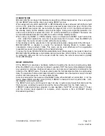
STANDBY MODE
MX29LV320AT/B can be set into Standby mode with two different approaches. One is using both
CE and RESET pins and the other one is using RESET pin only.
When using both pins of CE and RESET, a CMOS Standby mode is achieved with both pins held
at Vcc ±0.3V. Under this condition, the current consumed is less than 0.2uA (typ.). If both of the
CE and RESET are held at VIH, but not within the range of VCC ± 0.3V, the device will still be in
the standby mode, but the standby current will be larger. During Auto Algorithm operation, Vcc
active current (ICC2) is required even CE = "H" until the operation is completed. The device can
be read with standard access time (tCE) from either of these standby modes.
When using only RESET, a CMOS standby mode is achieved with RESET input held at Vss
0.3V, Under this condition the current is consumed less than 1uA (typ.). Once the RESET pin
is taken high, the device is back to active without recovery delay.
In the standby mode the outputs are in the high impedance state, independent of the OE input.
MX29LV320AT/B is capable to provide the Automatic Standby Mode to restrain power
consumption during readout of data. This mode can be used effectively with an application
requested low power consumption such as handy terminals.
To active this mode, MX29LV320AT/B automatically switch themselves to low power mode when
MX29LV320AT/B addresses remain stable during access time of tACC+30ns. It is not necessary
to control CE, WE, and OE on the mode. Under the mode, the current consumed is typically
0.2uA (CMOS level).
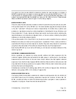
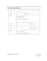
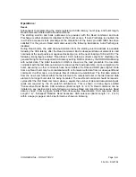
RESET OPERATION
01The RESET pin provides a hardware method of resetting the device to reading array data.
When the RESET pin is driven low for at least a period of tRP, the device immediately terminates
any operation in progress, tristates all output pins, and ignores all read/write commands for the
duration of the RESET pulse. The device also resets the internal state machine to reading array
data. The operation that was interrupted should be reinitiated once the device is ready to accept
another command sequence, to ensure data integrity.
Current is reduced for the duration of the RESET pulse. When RESET is held at VSS
0.3V, the
device draws CMOS standby current (ICC4). If RESET is held at VIL but not within VSS
0.3V,
the standby current will be greater.
The RESET pin may be tied to system reset circuitry. A system reset would that also reset the
Flash memory, enabling the system to read the boot-up firm-ware from the Flash memory.
If RESET is asserted during a program or erase operation, the RY/BY pin remains a "0" (busy)
until the internal reset operation is complete, which requires a time of tREADY (during
Embedded Algorithms).
Содержание VIZIO P42HDTV10A
Страница 1: ......
Страница 27: ...CONFIDENTIAL DO NOT COPY Page 6 3 File No SG 0184 Main Board Block Diagram ...
Страница 42: ...CONFIDENTIAL DO NOT COPY Page 8 10 File No SG 0184 DDR SDRAM M13S128168A 6T Application Pin description ...
Страница 60: ...CONFIDENTIAL DO NOT COPY Page 8 28 File No SG 0184 ...
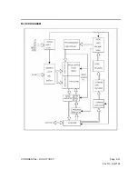
Страница 61: ...CONFIDENTIAL DO NOT COPY Page 8 29 File No SG 0184 BLOCK DIAGRAM ...
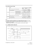
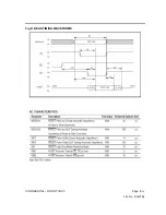
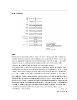
Страница 68: ...CONFIDENTIAL DO NOT COPY Page 8 36 File No SG 0184 Fig D READ TIMING WAVEFORMS ...
Страница 69: ...CONFIDENTIAL DO NOT COPY Page 8 37 File No SG 0184 Fig E RESET TIMING WAVEFORM ...
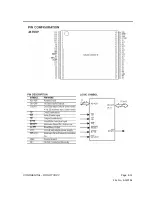
Страница 72: ...CONFIDENTIAL DO NOT COPY Page 8 40 File No SG 0184 Pin Configuration 400mil TSOP II x4 x8 x16 ...
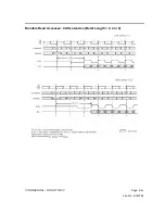
Страница 78: ...CONFIDENTIAL DO NOT COPY Page 8 46 File No SG 0184 Random Read Accesses CAS Latencies Burst Length 2 4 or 8 ...
Страница 94: ...CONFIDENTIAL DO NOT COPY Page 9 2 File No SG 0184 3 5V DV50A CB15 4 3 3V DV33A U5 3 ...
Страница 95: ...CONFIDENTIAL DO NOT COPY Page 9 3 File No SG 0184 5 2 5V DV25 CE42 6 1 8V DV18A U5 2 ...
Страница 97: ...CONFIDENTIAL DO NOT COPY Page 9 5 File No SG 0184 3 Sil 9011 Clock Ch1 U16 85 XTLI Ch2 U16 84 XTLO ...
Страница 99: ...CONFIDENTIAL DO NOT COPY Page 9 7 File No SG 0184 ATSC Board 1 Voltage Measurement 1 12V 12V C4 2 5V 5V C239 ...
Страница 100: ...CONFIDENTIAL DO NOT COPY Page 9 8 File No SG 0184 3 3 3V DV33 C11 4 2 5V DV25 C185 ...
Страница 101: ...CONFIDENTIAL DO NOT COPY Page 9 9 File No SG 0184 5 1 8V DV18 C64 6 1 25V 1V25_DDR C148 ...
Страница 102: ...CONFIDENTIAL DO NOT COPY Page 9 10 File No SG 0184 7 1 2V DV12 C26 ...
Страница 111: ...CONFIDENTIAL DO NOT COPY Page 10 7 File No SG 0184 TROUBLE OF THE DTV ...
Страница 196: ......
Страница 197: ......
Страница 198: ......
Страница 199: ......
Страница 200: ......
Страница 201: ......
Страница 202: ...CAM Products 2000 TM smbot art bot art ...
Страница 203: ...C ...
Страница 204: ...C ...
Страница 205: ...CAM350 V 7 6 Tue Feb 07 05 50 42 2006 Untitled VCC SCH ...
Страница 206: ...CAM350 V 7 6 Tue Feb 07 05 50 48 2006 Untitled Board ...
Страница 207: ...CAM350 V 7 6 Tue Feb 07 05 50 50 2006 Untitled BotSilk ...
Страница 208: ...CAM350 V 7 6 Tue Feb 07 05 50 51 2006 Untitled GND ...
Страница 209: ...CAM350 V 7 6 Tue Feb 07 05 50 53 2006 Untitled Board ...
Страница 210: ...CAM350 V 7 6 Tue Feb 07 05 50 54 2006 Untitled TopSilk ...
Страница 211: ...CAM350 V 7 6 Tue Feb 07 05 50 55 2006 Untitled VCC ...
Страница 212: ......
Страница 213: ......
Страница 214: ......
Страница 215: ......
Страница 216: ......
Страница 217: ......
Страница 218: ......
Страница 219: ......

