CONFIDENTIAL – DO NOT COPY
Page 8-
14
File No. SG-0184
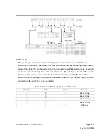
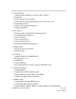
4. Row Active
The Bank Activation command is issued by holding CAS and WE high with CS and RAS low at
the rising edge of the clock (CLK). The DDR SDRAM has four independent banks; so two
Bank Select addresses (BA0, BA1) are required. The Bank Activation command to the first
read or write command must meet or exceed the minimum of RAS to CAS delay time (tRCD
min). Once a bank has been activated, it must be precharged before another Bank Activation
command can be applied to the same bank. The minimum time interval between interleaved
Bank Activation command (Bank A to Bank B and vice versa) is the Bank-to-Bank delay time
(tRRD min).
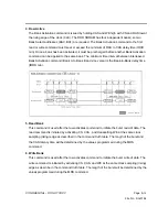
5. Read Bank
This command is used after the row activates command to initiate the burst read of data. The
read command is initiated by activating CS, CAS , and deasserting WE at the same clock
sampling (rising) edge as described in the command truth table. The length of the burst and
the CAS latency time will be determined by the values programmed during the MRS
command.
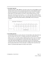
6. Write Bank
This command is used after the row activates command to initiate the burst write of data. The
write command is initiated by activating CS, CAS, and WE at the same clock sampling (rising)
edge as describe in the command truth table. The length of the burst will be determined by the
values programmed during the MRS command.
Содержание VIZIO P42HDTV10A
Страница 1: ......
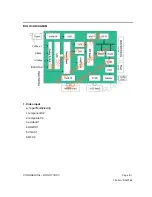
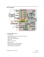
Страница 27: ...CONFIDENTIAL DO NOT COPY Page 6 3 File No SG 0184 Main Board Block Diagram ...
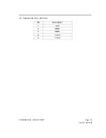
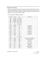
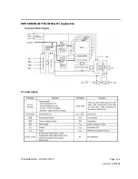
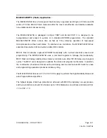
Страница 42: ...CONFIDENTIAL DO NOT COPY Page 8 10 File No SG 0184 DDR SDRAM M13S128168A 6T Application Pin description ...
Страница 60: ...CONFIDENTIAL DO NOT COPY Page 8 28 File No SG 0184 ...
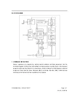
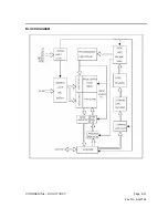
Страница 61: ...CONFIDENTIAL DO NOT COPY Page 8 29 File No SG 0184 BLOCK DIAGRAM ...
Страница 68: ...CONFIDENTIAL DO NOT COPY Page 8 36 File No SG 0184 Fig D READ TIMING WAVEFORMS ...
Страница 69: ...CONFIDENTIAL DO NOT COPY Page 8 37 File No SG 0184 Fig E RESET TIMING WAVEFORM ...
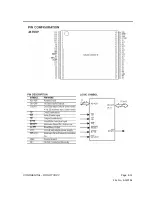
Страница 72: ...CONFIDENTIAL DO NOT COPY Page 8 40 File No SG 0184 Pin Configuration 400mil TSOP II x4 x8 x16 ...
Страница 78: ...CONFIDENTIAL DO NOT COPY Page 8 46 File No SG 0184 Random Read Accesses CAS Latencies Burst Length 2 4 or 8 ...
Страница 94: ...CONFIDENTIAL DO NOT COPY Page 9 2 File No SG 0184 3 5V DV50A CB15 4 3 3V DV33A U5 3 ...
Страница 95: ...CONFIDENTIAL DO NOT COPY Page 9 3 File No SG 0184 5 2 5V DV25 CE42 6 1 8V DV18A U5 2 ...
Страница 97: ...CONFIDENTIAL DO NOT COPY Page 9 5 File No SG 0184 3 Sil 9011 Clock Ch1 U16 85 XTLI Ch2 U16 84 XTLO ...
Страница 99: ...CONFIDENTIAL DO NOT COPY Page 9 7 File No SG 0184 ATSC Board 1 Voltage Measurement 1 12V 12V C4 2 5V 5V C239 ...
Страница 100: ...CONFIDENTIAL DO NOT COPY Page 9 8 File No SG 0184 3 3 3V DV33 C11 4 2 5V DV25 C185 ...
Страница 101: ...CONFIDENTIAL DO NOT COPY Page 9 9 File No SG 0184 5 1 8V DV18 C64 6 1 25V 1V25_DDR C148 ...
Страница 102: ...CONFIDENTIAL DO NOT COPY Page 9 10 File No SG 0184 7 1 2V DV12 C26 ...
Страница 111: ...CONFIDENTIAL DO NOT COPY Page 10 7 File No SG 0184 TROUBLE OF THE DTV ...
Страница 196: ......
Страница 197: ......
Страница 198: ......
Страница 199: ......
Страница 200: ......
Страница 201: ......
Страница 202: ...CAM Products 2000 TM smbot art bot art ...
Страница 203: ...C ...
Страница 204: ...C ...
Страница 205: ...CAM350 V 7 6 Tue Feb 07 05 50 42 2006 Untitled VCC SCH ...
Страница 206: ...CAM350 V 7 6 Tue Feb 07 05 50 48 2006 Untitled Board ...
Страница 207: ...CAM350 V 7 6 Tue Feb 07 05 50 50 2006 Untitled BotSilk ...
Страница 208: ...CAM350 V 7 6 Tue Feb 07 05 50 51 2006 Untitled GND ...
Страница 209: ...CAM350 V 7 6 Tue Feb 07 05 50 53 2006 Untitled Board ...
Страница 210: ...CAM350 V 7 6 Tue Feb 07 05 50 54 2006 Untitled TopSilk ...
Страница 211: ...CAM350 V 7 6 Tue Feb 07 05 50 55 2006 Untitled VCC ...
Страница 212: ......
Страница 213: ......
Страница 214: ......
Страница 215: ......
Страница 216: ......
Страница 217: ......
Страница 218: ......
Страница 219: ......

