MAX-M5Q - Hardware Integration Manual
FTX-HW-13008
Objective Specification
Design
Page 19 of 40
4.1.4
Antenna micro strip
There are many ways to design wave-guides on printed circuit boards. A common factor to all is that calculation
of the electrical parameters is not straightforward. Freeware tools like AppCAD from Agilent or TXLine from
Applied Wave Research, Inc. are of great help in this regard. Download these tools from
and
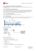
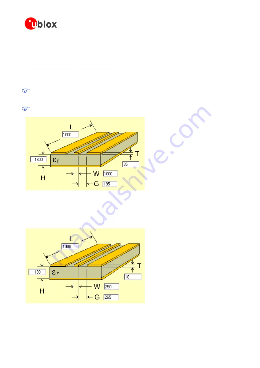
Micro strip is the most commonly used configuration on printed circuit boards; see Figure 10 and Figure 11. As a
rule of thumb, to achieve a 50
Ω
line impedance with FR-4 material, the width of the conductor is roughly
double the thickness of the dielectric.
For the correct calculation of the micro strip impedance, one does not only need to consider the
distance between the top and the first inner layer, but also the distance between the micro strip and the
adjacent GND plane on the same layer.
Use the Grounded Coplanar Waveguide model for the calculation of the line dimensions.
Figure 10: Micro strip on a 2-layer board (Agilent AppCAD Coplanar Waveguide)
Figure 10 shows an example of a 2-layer FR4 board with 1.6 mm thickness (
H
) and a 35 µm (1 ounce) copper
cladding (
T
). The thickness of the micro strip is comprised of the cladding (35 µm) plus the plated copper
(typically 25 µm). Figure 11 is an example of a multi layer FR4 board with 18 µm (½ ounce) cladding (
T
) and 180
µm dielectric between layer 1 and 2.
Figure 11: Micro strip on a multi layer board (Agilent AppCAD Coplanar Waveguide)

