


MAX-M5Q - Hardware Integration Manual
FTX-HW-13008
Objective Specification
Design
Page 18 of 40
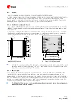
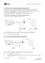
As seen in
an isolated ground area exists around and below the RF connection. This part of the circuit
MUST be kept as far from potential noise sources as possible. Make certain that no signal lines cross, and that no
signal trace vias appear at the PCB surface within the area of the red rectangle. The ground plane should also be
free of digital supply return currents in this area. On a multi layer board, the whole layer stack below the RF
connection should be kept free of digital lines. This is because even solid ground planes provide only limited
isolation.
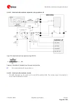
The impedance of the antenna connection must match the 50
Ω
impedance of the receiver. To achieve an
impedance of 50
Ω
, the width W of the micro strip has to be chosen depending on the dielectric thickness H,
the dielectric constant
ε
r
of the dielectric material of the PCB and on the build-up of the PCB (see
section 4.1.4).
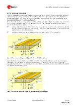
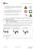
Figure 8 shows two different builds: A 2 Layer PCB and a four Layer PCB. The reference ground plane is in both
designs on layer 2 (red). Therefore, the effective thickness of the dielectric is different.
Module
micro strip line
Ground plane
Module
micro strip line
Ground plane
PCB
PCB
Either don't use these layers or fill with ground planes
H
H
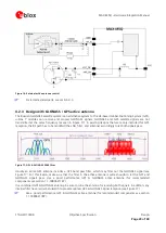
Figure 8: PCB build-up for micro strip line. Left: 2-layer PCB, right: 4-layer PCB
4.1.3
General design recommendations:
•
Keep the length of the micro strip line as short as possible. Avoid lengths over 2.5 cm (1 inch) on standard
PCB material and without additional shielding.
•
For multi-layer boards, the distance between micro strip line and ground area on the top layer should at
least be as large as the dielectric thickness.
•
Avoid routing the RF connection close to digital sections of the design.
•
To reduce signal reflections, avoid sharp angles in the routing of the micro strip line. Chamfers or fillets are
preferred for rectangular routing; 45-degree routing is preferred over Manhattan style 90-degree routing.
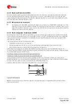
A
nte
nn
a
A
nte
nn
a
A
nte
nn
a
PCB
PCB
PCB
1
2
3
4
5
6
7
8
9
10
11
12
13
14
28
27
26
25
24
23
22
21
20
19
18
17
16
15
1
2
3
4
5
6
7
8
9
10
11
12
13
14
28
27
26
25
24
23
22
21
20
19
18
17
16
15
1
2
3
4
5
6
7
8
9
10
11
12
13
14
28
27
26
25
24
23
22
21
20
19
18
17
16
15
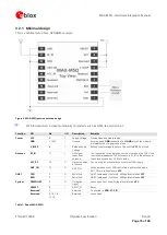
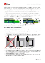
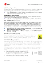
Wrong
better
best
Figure 9: Recommended micro strip routing to RF pin (for exact pin orientation see data sheet)
•
Do not route the RF-connection underneath the receiver. The distance of the micro strip line to the ground
plane on the bottom side of the receiver is very small (some 100 µm) and has huge tolerances (up to 100%).
Therefore, the impedance of this part of the trace cannot be controlled.
•
Use as many vias as possible to connect the ground planes.
•
In order to avoid reliability hazards, cover the area on the PCB under the receiver entirely with solder mask.
Vias should not be open. Do not route under the receiver.


