


MAX-M5Q - Hardware Integration Manual
FTX-HW-13008
Objective Specification
Design
Page 15 of 40
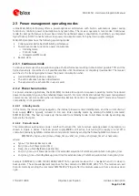
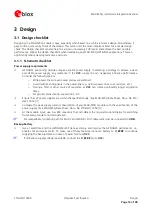
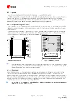
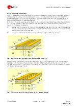
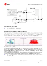
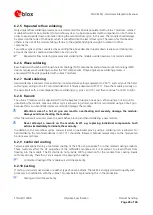
3.2.1
Minimal design
This is a minimal setup for a GPS/GNSS receiver:
Figure 3: MAX-M5Q passive antenna design
For information on increasing immunity to jammers such as GSM, see section 6.3.7.
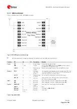
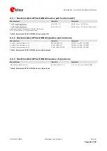
Function
PIN
No
I/O
Description
Remarks
Power
VCC
8
I
Supply Voltage
Provide clean and stable supply.
GND
1,10,12
I
Ground
Assure a good
GND
connection to all
GND
pins of the module,
preferably with a large ground plane.
V_BCKP
6
I
Backup Supply
Voltage
Backup supply voltage input pin. Connect to
VCC
if not used.
Antenna
RF_IN
11
I
GPS signal
input from
antenna
The connection to the antenna has to be routed on the PCB. Use a
controlled impedance of 50
Ω
to connect RF_IN
to the antenna or
the antenna connector. DC block inside.
VCC_RF
14
O
Output Voltage
RF section
Can be used for active antenna or external LNA supply.
ANT_ON
13
O
ANT_ON
Active antenna or ext. LNA control pin in power save mode.
ANT_ON pin voltage level is
VCC
UART
TXD
2
O
Serial Port
UART, leave open if not used, Voltage level referred
VCC
.
RXD
3
I
Serial Port
UART, leave open if not used, Voltage level referred
VCC
System
TIMEPULSE
4
O
Timepulse
Signal
Leave open if not used, Voltage level referred
VCC
VRESET
9
I
RESET_N
Reset
Reserved
7
-
Reserved
Connected to
VDD
(
VCC_IO
)
Reserved
5, 15, 16,
17, 18
-
Reserved
Leave open
Table 1: Pinout MAX-M5Q


