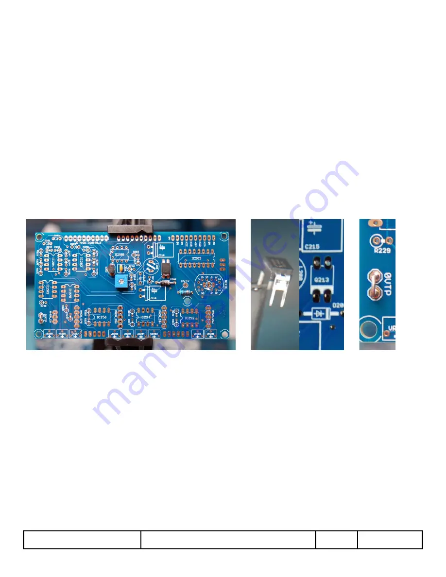
3-2) There are three major sections of circuitry on the Signal PCB. Input Signal Conditioning, Output Signal Conditioning, and the Voltage
Boost Circuit for the Nixie Tube anode. Building the Voltage Boost Circuit frst, allows us to test and calibrate it before installing the rest of
the components.
First, install Q212 [KSP42TA], Q213 [IRFD320], D200 [UF4004], C216 [2.2nF, 100V], R242 [6.8kΩ], and VR_HV [1kΩ] into the PCB and
solder them in place. Take care to not overheat Q212, Q213, and D200 while soldering. Also, don't forget to align the stripe on D200 with the
stripe on its component outline on the PCB. Align Q212 so that the fat side of the component matches the fat side of the component outline
on the PCB.
Take notice that the two DRAIN pins on Q213 are connected externally (the two pins on the other side are not connected). These two pins
match up with the stripe on the component outline on the PCB [below the text “Q213”]. Trim the leads for Q212, Q213, and D200 – Save one
of the trimmed leads from D200. Be sure to refow the solder on the Q212, Q213, and D200 pins after you trim them.
Take the trimmed lead that you saved from D200 to use as a jumper for the 0VDC Test Point [0VTP]. This will allow you to clip your meter's
COM lead to the PCB, freeing both hands for calibrating the output voltage of the Voltage Boost Circuit in Step 3-8. Bend one of these lead
clippings in the middle and insert them into the two solder pads of 0VTP and solder in place. Discard the other lead clipping:
DIY Build DOC/BOM
KOSMODROM CHAOS DIVIDER
V 1.4
Page 16


