background image


User's Manual  l  MBLS1028A UM 0100  l  © 2020, TQ-Systems GmbH 


Page  11 


4.2


Power supply 

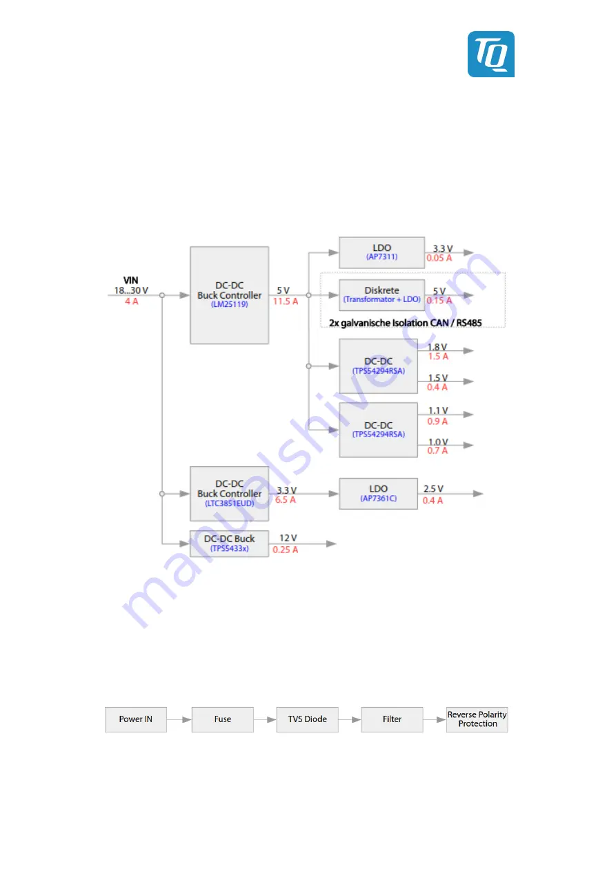
The MBLS1028A has to be supplied with 18 V to 28 V at X3 or X27. The typical supply voltage is 24 V. 
The following figure shows all voltages present on the MBLS1028A, which are structured into three main paths consisting of an 

LM25119, an LTC3851 and a TPS54335. These supply the biggest loads (TQMLS1028A, USB supply, SATA supply with up to 

2500 mA). The power supply structure is designed in such a way that the 5 V voltage is always activated. 
Furthermore the design allows power sequencing of all voltage levels used. All voltages are powered up after the boot process of 

the TQMLS1028A. 
At the two headers X25 and X38 on the MBLS1028A 1.8 V, 3.3 V, 5 V and 12 V are available. Both connectors share the available 

total power of the individual voltage rails. 


Figure 6: 

Block diagram power supply 


4.2.1


Protective circuitry 

The protection circuit (see Figure 7) features the following characteristics: 


Overcurrent protection by fuse 5 A, slow blow 


Overvoltage protection diode 


PI filter 


Reverse polarity protection by MOSFET 


Figure 7: 

Block diagram protective circuit 


4.2.2


Battery 

In case of power failure a lithium battery type CR2032 on the MBLS1028A supplies the RTC on the TQMLS1028A. 
 

Содержание MBLS1028A

Страница 1: ...MBLS1028A User s Manual MBLS1028A UM 0100 03 11 2020 ...

Страница 2: ...1 1 2 TQMLS1028A connectors 6 4 1 1 3 Boot configuration 6 4 1 2 Clock generation 7 4 1 3 Reset structure 8 4 1 4 I2 C devices 9 4 1 4 1 Temperature sensor 10 4 1 4 2 GPIO port expander 10 4 2 Power supply 11 4 2 1 Protective circuitry 11 4 2 2 Battery 11 4 3 Communication interfaces 12 4 3 1 Ethernet 12 4 3 1 1 RGMII 12 4 3 1 2 SGMII 12 4 3 1 3 QSGMII 13 4 3 2 USB 3 0 Hub 14 4 3 3 USB 3 0 OTG 15 ...

Страница 3: ...7 SAFETY REQUIREMENTS AND PROTECTIVE REGULATIONS 34 7 1 EMC 34 7 2 ESD 34 7 3 Operational safety and personal security 34 8 CLIMATIC AND OPERATIONAL CONDITIONS 34 8 1 Protection against external effects 34 8 2 Reliability and service life 34 9 ENVIRONMENT PROTECTION 35 9 1 RoHS 35 9 2 WEEE 35 9 3 REACH 35 9 4 EuP 35 9 5 Packaging 35 9 6 Batteries 35 9 6 1 General notes 35 9 6 2 Lithium batteries 3...

Страница 4: ...29 16 Table 12 CAN termination DIP switch S1 16 Table 13 Maximum permitted currents Mini PCIe X12 17 Table 14 Pinout Mini PCIe X12 18 Table 15 Pinout SIM card connector X13 18 Table 16 Pinout M 2 B Key X35 20 Table 17 Pinout mikroBUS connectors X32 X33 21 Table 18 Pinout SD card X16 22 Table 19 Pinout Header 1 X25 23 Table 20 Pinout Header 2 X38 24 Table 21 Pinout display port X15 25 Table 22 Supp...

Страница 5: ... Gbit ETH connectors X6 X7 12 Figure 11 Block diagram Ethernet QSGMII 13 Figure 12 Gbit ETH connectors X8 X9 13 Figure 13 Block diagram USB 3 0 Hub 14 Figure 14 Block diagram USB 15 Figure 15 Block diagram CAN 16 Figure 16 Block diagram Mini PCIe SIM card 17 Figure 17 Block diagram M 2 SSD SATA 19 Figure 18 Block diagram SD card 22 Figure 19 Block diagram display port 25 Figure 20 Block diagram JT...

Страница 6: ... trademarks are rightly protected by a third party 1 3 Disclaimer TQ Systems GmbH does not guarantee that the information in this User s Manual is up to date correct complete or of good quality Nor does TQ Systems GmbH assume guarantee for further usage of the information Liability claims against TQ Systems GmbH referring to material or non material related damages caused due to usage or non usage...

Страница 7: ...l used This symbol represents important details or aspects for working with TQ products Command A font with fixed width is used to denote commands file names or menu items 1 7 Handling and ESD tips General handling of your TQ products The TQ product may only be used and serviced by certified personnel who have taken note of the information the safety regulations in this document and all related ru...

Страница 8: ...The manufacturer s specifications of the components used for example CompactFlash cards are to be taken note of They contain if applicable additional information that must be taken note of for safe and reliable operation These documents are stored at TQ Systems GmbH Chip errata It is the user s responsibility to make sure all errata published by the manufacturer of each component are taken note of...

Страница 9: ...A All TQMLS1028A interfaces which can be used are available on the MBLS1028A thus the features of the CPU LS1028A can be evaluated and software development for a TQMLS1028A based project can be started directly The MBLS1028A supports TQMLS1028A modules with an LS1017A LS1027A LS1018A or LS1028A CPU 3 TECHNICAL DATA 3 1 System architecture and functionality 3 1 1 Block diagram MBLS1028A Figure 1 Bl...

Страница 10: ...S1028A The TQMLS1028A with its LS1028A CPU is the central system component It provides DDR4 SDRAM eMMC NOR flash and an EEPROM All TQMLS1028A internal voltages are derived from the 5 V supply voltage Further information can be found in the TQMLS1028A User s Manual The available signals are routed to the MBLS1028A via two connectors On the MBLS1028A the interfaces provided by the TQMLS1028A are rou...

Страница 11: ...old 0 2 µm 40 C to 125 C The TQMLS1028A is held in the mating connectors on the TQMLS1028A by 240 pins with a retention force of approximately 24 N To avoid damaging the connectors of the MBLS1028A or the TQMLS1028A while removing the TQMLS1028A the use of the extraction tool MOZI8XX is strongly recommended 4 1 1 3 Boot configuration The boot mode of the TQMLS1028A is determined by the level of th...

Страница 12: ...LS1028A UM 0100 l 2020 TQ Systems GmbH Page 7 4 1 2 Clock generation The following figure shows which clocks are required on the TQMLS1028A and how they are generated Figure 3 Block diagram clock generation on MBLS1028A ...

Страница 13: ...LS1028A and the Reset button on the MBLS1028A are the control center This ensures that the Reset is enabled at the right time during power up Corresponding reset delays are handled by the TQMLS1028A The remaining PHYs hub and other reset capable components on the module are controlled by the I2 C expander Figure 4 Block diagram Reset structure ...

Страница 14: ... I2 C devices address mapping on TQMLS1028A and MBLS1028A Location I2 C bus Device Function 7 bit address Remark MBLS1028A IIC5 SI5338C Clock Generator 0x70 111 0000b Optional not connected TUSB8041 USB 3 0 Hub 0x44 100 0100b Optional not connected mPCIe Defined by customer X12 mikroBUS Defined by customer X32 IIC6 PCA9555 Port expander 0x25 010 0101b Device D43 3 3 V PCA9538 Port expander 0x70 11...

Страница 15: ...e circuit diagram In the initial state after power up all ports are set as input and the connected component is thus deactivated The following table shows the signals controlled by the port expanders Table 5 Function of Port Expanders Port Signal Dir Remark 8 port Expander PCA9538 D68 I2 C address 0x25 010 0101b IO_0 EC1_INT I IO_1 EC1_RESET O IO_2 SGMII_INT I IO_3 SGMII_RESET O IO_4 QSGMII_INT I ...

Страница 16: ...rmore the design allows power sequencing of all voltage levels used All voltages are powered up after the boot process of the TQMLS1028A At the two headers X25 and X38 on the MBLS1028A 1 8 V 3 3 V 5 V and 12 V are available Both connectors share the available total power of the individual voltage rails Figure 6 Block diagram power supply 4 2 1 Protective circuitry The protection circuit see Figure...

Страница 17: ... CPU is generated by a quartz oscillator The RGMII interface contains PHY reset and interrupt signals The PHY signals are routed to RJ 45 connector X6 Figure 8 Block diagram Ethernet RGMII 4 3 1 2 SGMII The LS1028A provides an Ethernet controller SGMII port 0 which is used as SGMII interface via SerDes Lane 0 On the MBLS1028A the interface provides a Gigabit Ethernet port The SGMII interface conta...

Страница 18: ...thernet controller but via SerDes and is implemented as QSGMII The QSGMII interface includes PHY reset and interrupt signals When looking at the MBLS1028A from outside X8 is on the left X9 is on the right Figure 11 Block diagram Ethernet QSGMII The following table shows the pinout of the Ethernet connectors X8 and X9 Table 6 Pinout Ethernet QSGMII RJ 45 connectors X8 X9 RJ 45 X8 X9 Left Right Left...

Страница 19: ...B Type A X10 Pin Pin name Signal Remark 1 VBUS_2 V_VBUS_DN2 100 µF to DGND EMI filter 2 D _2 USB_DN2_D Common Mode Choke in series 3 D _2 USB_DN2_D Common Mode Choke in series 4 GND_2 DGND 5 SSRX _2 USB_DN2_RX Common Mode Choke in series 6 SSRX _2 USB_DN2_RX Common Mode Choke in series 7 GND DRAIN_2 DGND 8 SSTX _2 USB_DN2_TX Common Mode Choke in series 100 nF AC coupling capacitor 9 SSTX _2 USB_DN...

Страница 20: ...and hardware used the effective read and write rates of the ports may vary The following table shows the pinout of USB OTG connector X5 Table 10 Pinout USB OTG X5 Pin Pin name Signal I O Remark 1 VBUS V_VBUS_USB1 P 100 µF to DGND EMI filter 2 D USB1_D_M I O Common Mode Choke in series 3 D USB1_D_P I O Common Mode Choke in series 4 ID USB1_ID I 5 GND DGND P 6 SSTX USB1_TX_M I O Common Mode Choke in...

Страница 21: ... CAN The following table shows the pinout of the CAN connectors Table 11 Pinout CAN X17 X29 CAN bus connector Pin Signal Direction Remark CAN1 X17 CAN2 X29 1 CAN_H I O Galvanically separated 2 CAN_L I O 3 GND_CAN P The CAN signals can be terminated with 120 Ω using the DIP switches S1 1 S1 2 Table 12 CAN termination DIP switch S1 DIP switch Interface ON OFF S1 1 CAN1 CAN1 terminated with 120 Ω CAN...

Страница 22: ...ards 50 95 mm 30 mm Any standard compliant Mini PCIe card can be used A SIM card holder is also provided Figure 16 Block diagram Mini PCIe SIM card The voltages provided for the Mini PCIe card must not exceed the currents specified in the following table Table 13 Maximum permitted currents Mini PCIe X12 Voltage Nominal value Imax V_3V3_PCIE 3 3 V 1 1 A V_1V5_PCIE 1 5 V 0 375 A ...

Страница 23: ...U PD default 10 kΩ PU DGND 21 22 MPCIE_RST Global Reset 0 Ω serial termination SD1_RX2_N 23 24 V_3V3_MPCIE 0 Ω serial termination SD1_RX2_P 25 26 DGND DGND 27 28 V_1V5_MPCIE DGND 29 30 IIC5_SCL_MUX_A 100 nF in series SD1_TX2_N 31 32 IIC5_SDA_MUX_A I2 C address see Table 4 100 nF in series SD1_TX2_P 33 34 DGND DGND 35 36 USB_DN3_D DGND 37 38 USB_DN3_D V_3V3_MPCIE 39 40 DGND V_3V3_MPCIE 41 42 WWAN L...

Страница 24: ... mass storage Transfer rates of 1 5 Gb s Gen I 3 Gb s Gen II and 6Gb s Gen III are possible An M 2 slot with B coding is used on the MBLS1028A The MBLS1028A supports M 2 sizes 2242 2260 and 2280 The standard mounting is for type 2280 The SATA interface of the LS1028A and a 3 3 V power supply are connected to X35 According to the M 2 specification the power budget of the MBLS1028A includes 2 5 A fo...

Страница 25: ...G0 21 20 NC NC 23 22 NC NC 25 24 NC DGND 27 26 NC NC 29 28 NC NC 31 30 NC DGND 33 32 NC NC 35 34 NC NC 37 36 NC DGND 39 38 NC 10 nF AC from TQMLS1028A SD1_RX3_P 41 40 NC 10 nF AC from TQMLS1028A SD1_RX3_N 43 42 NC DGND 45 44 NC SD1_TX3_N 47 46 NC SD1_TX3_P 49 48 NC DGND 51 50 PERST 100 kΩ PU or 0 Ω PD default NP NC 53 52 NC NC 55 54 NC DGND 57 56 NC NC 59 58 NC NC 61 60 NC NC 63 62 NC NC 65 64 NC ...

Страница 26: ...e power consumption Since these are low power modules the current consumption is limited to 500 mA per supply rail The following table shows the signals of mikroBUS connectors X32 and X33 Table 17 Pinout mikroBUS connectors X32 X33 X33 X32 Remark Signal Name Pin Pin Name Signal Remark 10 kΩ to DGND optional 10 kΩ to 3 3 V 0 V AN 1 1 PWM Mikro_Module_PWM Mikro_Module_RST RST 2 2 INT Mikro_Module_IN...

Страница 27: ...rd Table 18 Pinout SD card X16 Pin Signal Remark 1 SDHC1_DATA2_R 10 kΩ PU to 3 3 V ESD protection 2 SDHC1_DATA3_R 10 kΩ PU to 3 3 V ESD protection 3 SDHC1_CMD_R 10 kΩ PU to 3 3 V ESD protection 4 VCC3V3 Optional 1 8 V or 3 3 V 5 SDHC1_CLK ESD protection 6 DGND 7 SDHC1_DATA0_R 10 kΩ PU to 3 3 V ESD protection 8 SDHC1_DATA1_R 10 kΩ PU to 3 3 V ESD protection SW1 SDHC1_CD 10 kΩ PU to 1 8 V ESD protec...

Страница 28: ...ystem RTC_CLKOUT 17 18 TA_PROG_SFP Factory Test 0 V Power DGND 19 20 TA_BB_VDD Power VDD 1 8 V XSPI XSPI1_A_SCK 21 22 DGND Power 0 V 0 V Power DGND 23 24 XSPI1_A_DATA4 XSPI 1 8 V 1 8 V XSPI XSPI1_A_DQS 25 26 XSPI1_A_DATA5 XSPI 1 8 V 0 V Power DGND 27 28 XSPI1_A_DATA6 XSPI 1 8 V 1 8 V XSPI XSPI1_A_DATA0 29 30 XSPI1_A_DATA7 XSPI 1 8 V 1 8 V XSPI XSPI1_A_DATA1 31 32 XSPI1_A_CS0 XSPI 1 8 V 1 8 V XSPI ...

Страница 29: ...ND 13 14 IIC1_SDA I2 C 1 8 V 1 8 V UART UART2_SIN_MUX_A 15 16 DGND Power 0 V 1 8 V UART UART2_SOUT_MUX_A 17 18 TEMP_ALERT System 3 3 V 0 V Power DGND 19 20 TEMP_CRIT_MOD System 3 3 V 1 8 V Reset PORESET 21 22 DGND Power 0 V 1 8 V Reset HRESET 23 24 CLK_OUT System VBAT 1 8 V Reset RESET_REQ 25 26 DGND Power 0 V 0 V Power DGND 27 28 ASLEEP Debug 1 8 V 0 V Power DGND 29 30 TA_TMP_DETECT Trust 1 8 V U...

Страница 30: ...pre emphasis level via software Figure 19 Block diagram display port Table 21 Pinout display port X15 Pin Signal Remark 1 DP_ML0 ESD protection 100 nF in series 2 DGND 3 DP_ML0 ESD protection 100 nF in series 4 DP_ML1 ESD protection 100 nF in series 5 DGND 6 DP_ML1 ESD protection 100 nF in series 7 DP_ML2 ESD protection 100 nF in series 8 DGND 9 DP_ML2 ESD protection 100 nF in series 10 DP_ML3 ESD...

Страница 31: ...ton S7 is provided on the MBLS1028A 4 4 5 User push button Two push buttons S4 S5 are provided on the MBLS1028A The push button status can be read at the 16 port I2 C expander PCA9538 D69 see Table 5 4 4 6 DIP switches Two 4 fold DIP switches S9 S10 are provided on the MBLS1028A The function of DIP switch S9 is described in Table 3 With DIP switch S10 the SPI IIC5 UART2 and VCC_FAN signals on the ...

Страница 32: ...e OpenSDA circuitry see chapter 4 5 2 A Lauterbach debugger is intended for programming the TQMLS1028A The JTAG interface has no ESD protection Figure 20 Block diagram JTAG The following table shows the pin assignment of the JTAG connector Table 24 Pinout JTAG header X34 Pin Signal Remark 1 JTAG_VREF 100 Ω in series to 1 8 V use only as reference 2 1 8 V 0 Ω in series to 1 8 V 3 JTAG_TRST 10 kΩ PU...

Страница 33: ...or X24 to connect to a PC is available The following table shows the pin assignment of the JTAG connector for the Kinetis µC D23 Table 25 Pinout OpenSDA 100 mil header X22 Pin Signal Remark 1 V_SDA_3V3 2 SDA_JTAG_TMS 10 kΩ PU to V_SDA_3V3 OpenSDA interface 3 DGND 4 SDA_JTAG_TCLK 5 DGND 6 SDA_JTAG_TDO 7 NC 8 SDA_JTAG_TDI 9 DGND 10 SDA_RESET Table 26 Pinout OpenSDA USB Mini B X24 Pin Signal Remark 1...

Страница 34: ... AB connector X19 To use the UART a DIP switch S8 is provided to switch off the USB path Figure 21 Block diagram Debug RS 232 Table 27 Pinout Debug USB X19 Pin Signal 1 V_USB_DBG_VBUS 2 USB_DBG_D 3 USB_DBG_D 4 NC 5 DGND M1 M6 DGND 5 SOFTWARE No software is required for the MBLS1028A Suitable software is only required on the TQMLS1028A and is not a part of this specification More information can be...

Страница 35: ...MBLS1028A has overall dimensions length width of 170 170 mm2 The MBLS1028A has a maximum height of approximately 26 4 mm The MBLS1028A has six 4 3 mm mounting holes for the housing and four 3 2 mm mounting holes for a heat sink The MBLS1028A weighs approximately 200 grams without TQMLS1028A Figure 22 MBLS1028A dimensions ...

Страница 36: ... installation in a standard EURO housing 6 5 Thermal management The MBLS1028A has a maximum peak power consumption of approximately 3 watts Further power loss occurs mainly at externally connected devices Attention TQMLS1028A heat dissipation The LS1028A CPU belongs to a performance category in which a cooling system is essential It is the user s sole responsibility to define a suitable heat sink ...

Страница 37: ... GmbH Page 32 6 6 Assembly Figure 23 MBLS1028A component placement top The labels on the MBLS1028A revision 0100 show the following information Table 28 Labels on MBLS1028A Label Text AK1 Serial number AK2 MBLS1028A version and revision tests performed ...

Страница 38: ...User s Manual l MBLS1028A UM 0100 l 2020 TQ Systems GmbH Page 33 6 6 Assembly continued Figure 24 MBLS1028A component placement bottom ...

Страница 39: ...storing 10 to 90 Not condensing Attention TQMLS1028A heat dissipation The LS1028A CPU belongs to a performance category in which a cooling system is essential It is the user s sole responsibility to define a suitable heat sink weight and mounting position depending on the specific mode of operation e g dependence on clock frequency stack height airflow and software Particularly the tolerance chain...

Страница 40: ...ies are generally only mounted in sockets 9 6 2 Lithium batteries The requirements concerning special provision 188 of the ADR section 3 3 are complied with for Lithium batteries There is therefore no classification as dangerous goods Basic lithium content per cell not more than 1 grams except for lithium ion and lithium polymer cells for which a lithium content of not more than 1 5 g per cell app...

Страница 41: ...ility EMI Electromagnetic Interference eMMC embedded Multimedia Card flash ESD Electrostatic Discharge EuP Energy using Products FR 4 Flame Retardant 4 GPIO General Purpose Input Output GPU Graphics Processing Unit I Input I O Input Output I2C Inter Integrated Circuit IEEE Institute of Electrical and Electronics Engineers IIC Inter Integrated Circuit IP00 Ingress Protection 00 JTAG Joint Test Acti...

Страница 42: ...HS Restriction of the use of certain Hazardous Substances RS 232 Recommended Standard serial interface RTC Real Time Clock SATA Serial Advanced Technology Attachment SD Secure Digital SDHC Secure Digital High Capacity SDRAM Synchronous Dynamic Random Access Memory SerDes Serializer Deserializer SGMII Serial Gigabit Media Independent Interface SIM Subscriber Identification Module SPI Serial Periphe...

Страница 43: ...her applicable documents No Name Rev Date Company 1 QorIQ LS1028A Data Sheet Rev 0 12 2019 NXP 2 QorIQ LS1028A Reference Manual Rev 0 12 2019 NXP 3 QorIQ LS1028A Design Checklist AN12028 Rev 0 12 2019 NXP 4 TQMLS1028A User s Manual current TQ Systems 5 TQMLS1028A Support Wiki current TQ Systems ...

Страница 44: ...TQ Systems GmbH Mühlstraße 2 l Gut Delling l 82229 Seefeld Info TQ Group TQ Group ...

Отзывы: