Page 159
TMP86PM29BUG
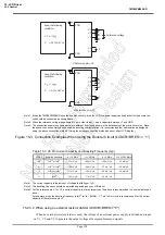
The smaller the external resistor value, the higher the segment/common drive capability, but power con-
sumption is increased. Conversely, the larger the external resistor value, the lower the segment/common
drive capability, but power consumption is reduced. If the drive capability is insufficient, the LCD may
not be displayed clearly. Therefore, select an optimum resistor value for the LCD panel to be used.
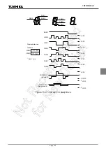
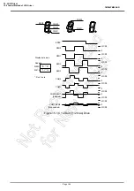
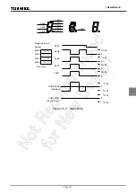
Figure 15-4 Connection Examples When Using an External Resistor Divider
(LCDCR<BRES> = “0”)
15.3 LCD Display Operation
15.3.1 Display data setting
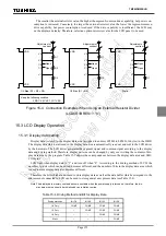
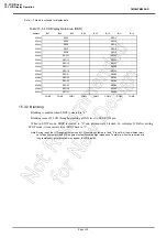
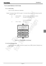
Display data is stored to the display data area (assigned to address 0F80H to 0F8FH, 16bytes) in the DBR.
The display data which are stored in the display data area is automatically read out and sent to the LCD driver
by the hardware. The LCD driver generates the segment signal and common signal according to the display
data and driving method. Therefore, display patterns can be changed by only over writing the contents of dis-
play data area by the program. Table 15-5 shows the correspondence between the display data area and SEG/
COM pins.
LCD light when display data is “1” and turn off when “0”. According to the driving method of LCD, the
number of pixels which can be driven becomes different, and the number of bits in the display data area which
is used to store display data also becomes different.
Therefore, the bits which are not used to store display data as well as the data buffer which corresponds to the
addresses not connected to LCD can be used to store general user process data (see Table 15-4).
Note:The display data memory contents become unstable when the power supply is turned on; therefore, the dis-
play data memory should be initialized by an initiation routine.
Table 15-4 Driving Method and Bit for Display Data
Driving methods
Bit 7/3
Bit 6/2
Bit 5/1
Bit 4/0
1/4 Duty
COM3
COM2
COM1
COM0
1/3 Duty
–
COM2
COM1
COM0
1/2 Duty
–
–
COM1
COM0
Static
–
–
–
COM0
Adjustment of
contrast
Adjustment of
contrast
Adjustment of
contrast
R3
R2
R1
Open
V3
V2
C0
C1
V1
VDD
VSS
Open
1/3 Bias (R1 = R2 = R3)
R2
R1
Open
V3
V2
C0
C1
V1
VDD
VSS
Open
R1
Open
V3
V2
C0
C1
V1
VDD
VSS
Open
Static
Keep the following conditon.
VDD V3 V2 V1 VSS
1/2 Bias (R1 = R2)
Содержание TLCS-870/C Series
Страница 1: ...8 Bit Microcontroller TLCS 870 C Series TMP86PM29BUG ...
Страница 6: ...TMP86PM29BUG ...
Страница 7: ...Revision History Date Revision 2007 10 11 1 First Release 2008 8 29 2 Contents Revised ...
Страница 9: ......
Страница 15: ...vi ...
Страница 19: ...Page 4 1 3 Block Diagram TMP86PM29BUG 1 3 Block Diagram Figure 1 2 Block Diagram ...
Страница 23: ...Page 8 1 4 Pin Names and Functions TMP86PM29BUG ...
Страница 48: ...Page 33 TMP86PM29BUG ...
Страница 49: ...Page 34 2 Operational Description 2 3 Reset Circuit TMP86PM29BUG ...
Страница 61: ...Page 46 3 Interrupt Control Circuit 3 8 External Interrupts TMP86PM29BUG ...
Страница 81: ...Page 66 6 Watchdog Timer WDT 6 3 Address Trap TMP86PM29BUG ...
Страница 135: ...Page 120 10 8 Bit TimerCounter TC5 TC6 10 1 Configuration TMP86PM29BUG ...
Страница 145: ...Page 130 11 Asynchronous Serial interface UART 11 9 Status Flag TMP86PM29BUG ...
Страница 165: ...Page 150 13 10 bit AD Converter ADC 13 6 Precautions about AD Converter TMP86PM29BUG ...
Страница 183: ...Page 168 15 LCD Driver 15 4 Control Method of LCD Driver TMP86PM29BUG ...
Страница 201: ...Page 186 18 Electrical Characteristics 18 9 Handling Precaution TMP86PM29BUG ...
Страница 203: ...Page 188 19 Package Dimensions TMP86PM29BUG ...
Страница 205: ......

