2 Setup
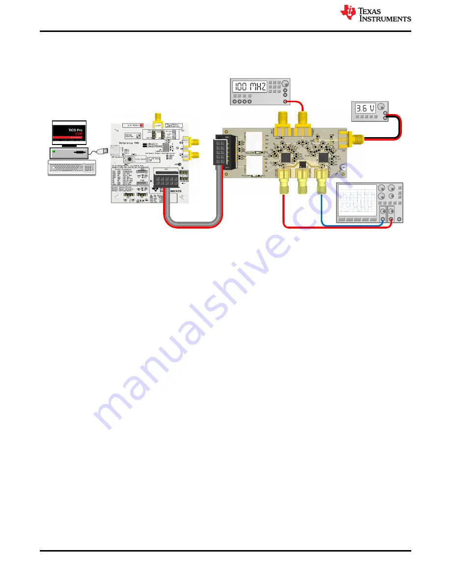
2.1 Connection Diagram
Figure 2-1. Connection Diagram
2.2 Power Supply
Apply 3.6 V to Vcc SMA connector. Acceptable supply voltage range is 3.5 V to 5 V. The maximum current
consumption in the most extreme configuration must not exceed 1200 mA. The onboard LDOs will provide a
3.3-V supply to the LMX2594 devices.
2.3 Reference Clock
Connect a low jitter reference clock to the OSCin SMA connector. This clock is evenly distributed to both
LMX2594 devices. If a sine wave clock is used, 8 dBm or more input power is suggested.
2.4 SYNC Input
In category 1 and 2 phase synchronization, the timing of the SYNC signal is not critical. This SYNC signal can
be generated from the Reference Pro board. In category 3 phase synchronization, the SYNC signal has to be
carefully aligned with the reference clock of the synthesizers. This SYNC signal shall be provided externally to
the SYNC SMA connector.
2.5 RF Output
Each LMX2594 device has two RF outputs, but only RFoutA is used. By default, RFoutAP pin is connected to
the SMA connector while the RFoutAM pin is terminated onboard. This is the default configuration to measure
the phases between the outputs of the LMX2594 devices. With some modification to the EVM, the sum of the
two LMX2594 devices output can be obtained from the SumRFout SMA connector. See
for more
information on EVM modification.
2.6 Programming
Connect the ribbon cable from the Reference PRO to the LMX2594PSEVM.
Connect the USB cable from a PC to the USB port on the Reference PRO board. This provides a power
supply to the Reference PRO board and communication with the TICS Pro software. A firmware update may be
required. See
for details.
The two LMX2594 devices share the uWIRE socket but only one device can be programmed at a time. Make
sure that only one of the DIP switches is in the ON position at a time.
Setup
4
LMX2594PSEVM Evaluation Instructions
SNAU278 – JULY 2022
Copyright © 2022 Texas Instruments Incorporated


