background image

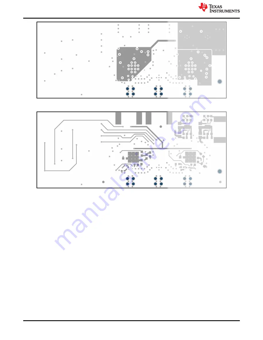
Figure 5-4. Power Layer

Figure 5-5. Bottom Layer

PCB Layout and Layer Stack-up

www.ti.com

12

LMX2594PSEVM Evaluation Instructions

SNAU278 – JULY 2022

Submit Document Feedback

Copyright © 2022 Texas Instruments Incorporated

Содержание LMX2594PSEVM

Страница 1: ...ithout using an internal doubler thus eliminating the need for sub harmonic filters Table of Contents 1 LMX2594PSEVM Evaluation Module 3 1 1 Evaluation Module Contents 3 1 2 Evaluation Setup Requirement 3 1 3 Resources 3 2 Setup 4 2 1 Connection Diagram 4 2 2 Power Supply 4 2 3 Reference Clock 4 2 4 SYNC Input 4 2 5 RF Output 4 2 6 Programming 4 2 7 Evaluation Software 5 3 Typical Measurement 6 3 ...

Страница 2: ...6 9 2 Output Format Selection 17 9 3 Typical Output Characteristics 18 9 4 Firmware Update 18 Trademarks PLLatinum is a trademark of Texas Instruments Windows is a registered trademark of Microsoft Corporation All trademarks are the property of their respective owners Trademarks www ti com 2 LMX2594PSEVM Evaluation Instructions SNAU278 JULY 2022 Submit Document Feedback Copyright 2022 Texas Instru...

Страница 3: ...ning Windows 7 or more recent version An oscilloscope A high quality signal generator Texas Instruments Clocks and Synthesizers TICS Pro software Texas Instruments PLLatinum Simulator Tool optional 1 3 Resources Related evaluation and development resources include LMX2594 data sheet TICS Pro software PLLatinum Simulator Tool PLL Sim Reference PRO design file Reference designs TIDA 01410 TIDA 01346...

Страница 4: ... 5 RF Output Each LMX2594 device has two RF outputs but only RFoutA is used By default RFoutAP pin is connected to the SMA connector while the RFoutAM pin is terminated onboard This is the default configuration to measure the phases between the outputs of the LMX2594 devices With some modification to the EVM the sum of the two LMX2594 devices output can be obtained from the SumRFout SMA connector ...

Страница 5: ... Run the software and follow the following steps to get started 1 Go to Select Device PLL VCO LMX2594 2 Go to Default Configuration Default Mode www ti com Setup SNAU278 JULY 2022 Submit Document Feedback LMX2594PSEVM Evaluation Instructions 5 Copyright 2022 Texas Instruments Incorporated ...

Страница 6: ...s critical Shown below is a category 3 synchronization example Figure 3 1 Category 3 TICS Pro Configuration If it is a category 3 synchronization VCO_PHASE_SYNC should be checked to put the devices in SYNC mode After programming the outputs from the two LMX2594 devices may not be phase aligned Figure 3 2 Output Phases Before Synchronization Typical Measurement www ti com 6 LMX2594PSEVM Evaluation ...

Страница 7: ...e to the output power being 6 dB higher while the noise power is only 3 dB higher To measure the combined phase noise some modification to the EVM is needed See Section 7 for details In Figure 3 5 the blue trace shown the phase noise of individual LMX2594 device while the black trace respresented the phase noise of the combined signal www ti com Typical Measurement SNAU278 JULY 2022 Submit Documen...

Страница 8: ...Figure 3 5 Combined Phase Noise Typical Measurement www ti com 8 LMX2594PSEVM Evaluation Instructions SNAU278 JULY 2022 Submit Document Feedback Copyright 2022 Texas Instruments Incorporated ...

Страница 9: ... 1 LMX2594PSEVM Schematic Page 1 Figure 4 2 LMX2594PSEVM Schematic Page 2 www ti com Schematic SNAU278 JULY 2022 Submit Document Feedback LMX2594PSEVM Evaluation Instructions 9 Copyright 2022 Texas Instruments Incorporated ...

Страница 10: ...Figure 4 3 LMX2594PSEVM Schematic Page 3 Schematic www ti com 10 LMX2594PSEVM Evaluation Instructions SNAU278 JULY 2022 Submit Document Feedback Copyright 2022 Texas Instruments Incorporated ...

Страница 11: ...0 mil FR4 Er 4 2 8 mil Bottom layer 62 mil Power layer Figure 5 1 PCB Layer Stack Up 5 2 PCB Layout Figure 5 2 Top Layer Figure 5 3 GND Layer www ti com PCB Layout and Layer Stack up SNAU278 JULY 2022 Submit Document Feedback LMX2594PSEVM Evaluation Instructions 11 Copyright 2022 Texas Instruments Incorporated ...

Страница 12: ...5 4 Power Layer Figure 5 5 Bottom Layer PCB Layout and Layer Stack up www ti com 12 LMX2594PSEVM Evaluation Instructions SNAU278 JULY 2022 Submit Document Feedback Copyright 2022 Texas Instruments Incorporated ...

Страница 13: ...ore 18 nH SMD LQG15HS18NJ02D MuRata R1 R2 R4_LF1 R4_LF2 R26 R30 R35 7 RES 0 5 0 1 W 0603 CRCW06030000Z0EA Vishay Dale R2_LF1 R2_LF2 2 RES 68 5 0 1 W 0603 CRCW060368R0JNEA Vishay Dale R3 R3_LF1 R3_LF2 R4 R5 R7 R8 R10 8 RES 18 5 0 1 W 0603 CRCW060318R0JNEA Vishay Dale R6 R9 R11 R14 R18 R27 R28 R31 R32 R33 R36 11 RES 12 k 5 0 1 W 0603 CRCW060312K0JNEA Vishay Dale R12 R13 2 RES 330 5 0 1 W 0603 RC0603...

Страница 14: ...luate the phase noise improvement by summing the two outputs together do the following modifications Move C13 to C13p Move C30 to C30p Figure 7 1 EVM Modification for Phase Noise Reduction EVM Modification www ti com 14 LMX2594PSEVM Evaluation Instructions SNAU278 JULY 2022 Submit Document Feedback Copyright 2022 Texas Instruments Incorporated ...

Страница 15: ...ake modifications to the EVM or change the default settings Register readback requires the correct hardware and software setup The POR current of the LMX2594PSEVM is approximately 400 mA Figure 8 1 Trouble Shooting Guide www ti com Troubleshooting Guide SNAU278 JULY 2022 Submit Document Feedback LMX2594PSEVM Evaluation Instructions 15 Copyright 2022 Texas Instruments Incorporated ...

Страница 16: ... position to the ground plane are connected by 1 5 kΩ resistors By default the board is configured for 100 MHz LVPECL output The power supply to Reference PRO is obtained from the PC through a USB connection Figure 9 1 Reference PRO Board 9 1 Output Frequency Selection Jumpers FS1 and FS0 are used to set the output frequency Table 9 1 Reference PRO Output Frequency Selection FS1 FS0 OUTPUT FREQUEN...

Страница 17: ... Ω R26 R29 150 Ω C24 C25 0 01 µF R27 R30 R31 DNP DC 1 R15 R28 C24 C25 0 Ω R26 R27 R29 R30 R31 DNP LVDS 2 AC R25 R27 R28 R30 0 Ω R31 100 Ω C24 C25 0 01 µF R26 R29 DNP DC R25 R27 R28 R30 C24 C25 0 Ω R31 100 Ω R26 R29 DNP HCSL AC R15 R28 0 Ω R26 R29 50 Ω C24 C25 0 01 µF R27 R30 R31 DNP DC R25 R28 C24 C25 0 Ω R26 R29 50 Ω R27 R30 R31 DNP 1 50 Ω to VCC 2 V termination is required on receiver 2 100 Ω di...

Страница 18: ... pop up instructions to complete the update This is necessary to ensure that the USB connection between the PC and the Reference PRO board is properly set up otherwise the programming to LMX2594PSEVM will not be successful 1 When you see this message press the OK button Figure 9 5 Firmware Requirement 2 Next follow the on screen procedure Reference PRO www ti com 18 LMX2594PSEVM Evaluation Instruc...

Страница 19: ...l the Update Fireware pop up appears Figure 9 8 Update Firmware 5 Press the Upgrade Firmware button to start the firmware upgrade Press the Close button after the upgrade is complete www ti com Reference PRO SNAU278 JULY 2022 Submit Document Feedback LMX2594PSEVM Evaluation Instructions 19 Copyright 2022 Texas Instruments Incorporated ...

Страница 20: ...e to check the USB connection in TICS Pro Make sure the USB Connected button is now green Figure 9 10 USB Communications Reference PRO www ti com 20 LMX2594PSEVM Evaluation Instructions SNAU278 JULY 2022 Submit Document Feedback Copyright 2022 Texas Instruments Incorporated ...

Страница 21: ...other than TI b the nonconformity resulted from User s design specifications or instructions for such EVMs or improper system design or c User has not paid on time Testing and other quality control techniques are used to the extent TI deems necessary TI does not test all parameters of each EVM User s claims against TI under this Section 2 are void if User fails to notify TI of any apparent defects...

Страница 22: ... These limits are designed to provide reasonable protection against harmful interference in a residential installation This equipment generates uses and can radiate radio frequency energy and if not installed and used in accordance with the instructions may cause harmful interference to radio communications However there is no guarantee that interference will not occur in a particular installation...

Страница 23: ...y for convenience and should be verified by User 1 Use EVMs in a shielded room or any other test facility as defined in the notification 173 issued by Ministry of Internal Affairs and Communications on March 28 2006 based on Sub section 1 1 of Article 6 of the Ministry s Rule for Enforcement of Radio Law of Japan 2 Use EVMs only after User obtains the license of Test Radio Station as provided in R...

Страница 24: ... any interfaces electronic and or mechanical between the EVM and any human body are designed with suitable isolation and means to safely limit accessible leakage currents to minimize the risk of electrical shock hazard User assumes all responsibility and liability for any improper or unsafe handling or use of the EVM by User or its employees affiliates contractors or designees 4 4 User assumes all...

Страница 25: ...OR DAMAGES ARE CLAIMED THE EXISTENCE OF MORE THAN ONE CLAIM SHALL NOT ENLARGE OR EXTEND THIS LIMIT 9 Return Policy Except as otherwise provided TI does not offer any refunds returns or exchanges Furthermore no return of EVM s will be accepted if the package has been opened and no return of the EVM s will be accepted if they are damaged or otherwise not in a resalable condition If User feels it has...

Страница 26: ...o change without notice TI grants you permission to use these resources only for development of an application that uses the TI products described in the resource Other reproduction and display of these resources is prohibited No license is granted to any other TI intellectual property right or to any third party intellectual property right TI disclaims responsibility for and you will fully indemn...

Отзывы: