V
OUT
V
+
V
±
+
V
B
AVDD
GND
AIN_nP
AIN_nGND
1
0
1
0
R
DC
R
FB
0V
V
P+
V
P-
R
S
ESD
D1p
D2n
R
S
AVDD
AVDD
D2p
D1n
ESD
SBAS582C – JULY 2014 – REVISED APRIL 2015
Feature Description (continued)
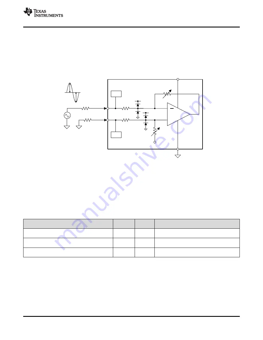
8.3.3 Input Overvoltage Protection Circuit
The ADS8684 and ADS8688 feature an internal overvoltage protection circuit on each of the four or eight analog
input channels, respectively. Use these protection circuits as a secondary protection scheme to protect the
device. TI highly recommends using external protection devices against surges, electrostatic discharge (ESD),
and electrical fast transient (EFT) conditions. The conceptual block diagram of the internal overvoltage protection
(OVP) circuit is shown in
Figure 52. Input Overvoltage Protection Circuit Schematic
As shown in
, the combination of the 1-M
Ω
input resistors along with the PGA gain-setting resistors
(R
FB
and R
DC
) limit the current flowing into the input pins. A combination of antiparallel diodes (D1 and D2) are
added on each input pin to protect the internal circuitry and set the overvoltage protection limits.
explains the various operating conditions for the device when the device is powered on.
indicates that when the AVDD pin of the device is connected to the proper supply voltage (AVDD = 5 V) or offers
a low impedance of < 30 k
Ω
, the internal overvoltage protection circuit can withstand up to ±20 V on the analog
input pins.
Table 1. Input Overvoltage Protection Limits When AVDD = 5 V or Offers a Low Impedance of < 30 k
Ω
(1)
INPUT CONDITION
TEST
ADC
COMMENTS
(V
OVP
= ±20 V)
CONDITION
OUTPUT
All input
|V
IN
| < |V
RANGE
|
Within operating range
Valid
Device functions as per data sheet specifications
ranges
Beyond operating range but
All input
ADC output is saturated, but device is internally
|V
RANGE
| < |V
IN
| < |V
OVP
|
Saturated
within overvoltage range
ranges
protected (not recommended for extended time)
All input
This usage condition may cause irreversible damage
|V
IN
| > |V
OVP
|
Beyond overvoltage range
Saturated
ranges
to the device
(1)
GND = 0, AIN_
n
GND = 0 V, |V
RANGE
| is the maximum input voltage for any selected input range, and |V
OVP
| is the break-down voltage
for the internal OVP circuit. Assume R
S
is approximately 0.
The results indicated in
are based on an assumption that the analog input pins are driven by very low
impedance sources (R
S
is approximately 0). However, if the sources driving the inputs have higher impedance,
the current flowing through the protection diodes reduces further, thereby increasing the OVP voltage range.
Note that higher source impedance results in gain errors and contributes to overall system noise performance.
Copyright © 2014–2015, Texas Instruments Incorporated
23
Product Folder Links:


