CLK IN
14bit
ADC
14bit
ADC
14bit
ADC
14bit
ADC
Digital
Block
+
Output
Formatter
DCLK
DAB P/M sLVDS
2
DCD P/M sLVDS
2
Power
Supply
Circuits
USB
To
SPI
5V
USB
ADC34xx
CH A
CH B
CH C
CH D
FCLK
Introduction
1.1
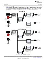
EVM Block Diagram
and
show a simplified block diagram of the default configuration of the EVM. The two or
four analog inputs are supplied to the EVM through a single-ended SMA connection, then transformer
coupled to turn the single ended signal into a balanced differential signal and then input to the ADC32xxx
or ADC34xxx. A dual transformer input circuit is used for better phase and amplitude balance of the input
signal than would typically be produced by a single transformer input circuit.
Figure 1. Simplified ADC344x EVM Block Diagram
4
ADC3xxx, ADC3xJxx EVM User’s Guide
SLAU579A – June 2014 – Revised September 2014
Copyright © 2014, Texas Instruments Incorporated


