TPMC533 User Manual Issue 1.0.1
Page 31 of 107
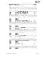
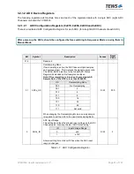
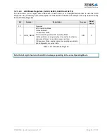
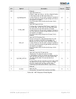
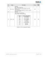
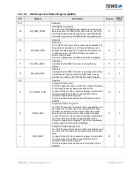
3.2.1.3.5
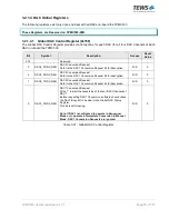
FIFO Level Register (0x134)
Bit
Symbol
Description
Access
Reset
Value
31:0
ADC_SEQ_FIFO_LEVEL
FIFO Level
This value shows the current fill level of the Sequencer's
internal FIFO. It is measured in number of bytes.
(an ADC Data value consists of two bytes)
R
0x0000
0000
Table 3-25: FIFO Level Register
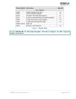
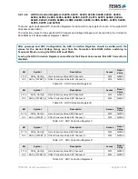
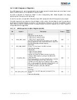
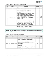
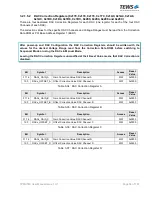
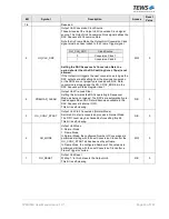
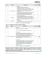
3.2.1.3.6
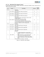
DMA Buffer Base Address Register (0x140)
Bit
Symbol
Description
Access
Reset
Value
31:0
WR_DMA_BUF_ADDR
DMA Buffer Base Address
PCI memory mapped base address of the DMA Buffer in
Host RAM where sampled ADC Data is written to.
The DMA Buffer Base Address is latched when the DMA
Buffer Length Register is written.
R/W
0x0000
0000
Table 3-26: DMA Buffer Base Address Register
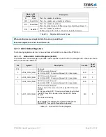
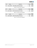
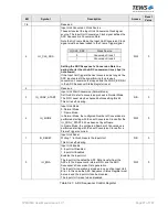
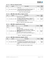
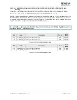
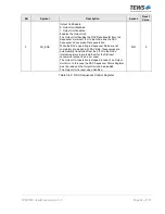
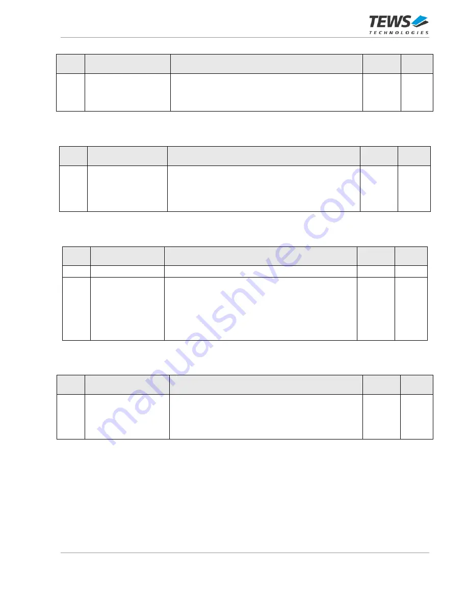
3.2.1.3.7
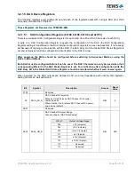
DMA Buffer Length Register (0x144)
Bit
Symbol
Description
Access
Reset
Value
31:28
-
Reserved
-
-
27:0
WR_DMA_BUF_LEN
DMA Buffer Length
Byte Length of the provided DMA Buffer in Host RAM.
A write to the DMA Buffer Length Register initiates the
DMA transfer.
The Initiation of DMA transfers is only possible if
WR_DMA_IDLE in the ADC Sequencer Status Register is
‘1’.
R/W
0x0000
0000
Table 3-27: DMA Buffer Length Register
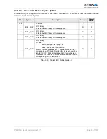
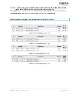
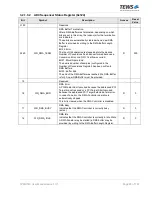
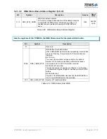
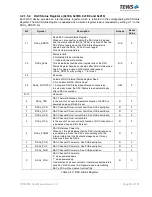
3.2.1.3.8
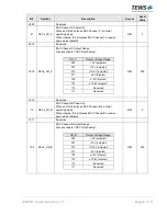
DMA Buffer Next Address Register (0x148)
Bit
Symbol
Description
Access
Reset
Value
31:0
WR_DMA_NEXT_ADDR
DMA Buffer Next Address
This register holds the PCI address of the address location
in Host RAM the next ADC Data is written to. It can be used
to determine how much space is left in the provided DMA
Buffer.
R
0x0000
0000
Table 3-28: DMA Buffer Next Address Register


