TPMC533 User Manual Issue 1.0.1
Page 26 of 107
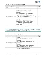
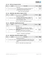
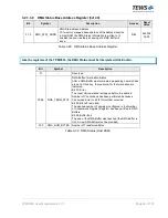
3.2.1.3 ADC Sequencer Registers
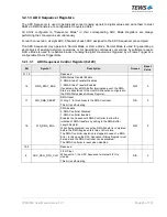
The ADC Sequencer is used to periodically convert analog signals to digital values and write them to Host
RAM via DMA transfers at a configurable Conversion Rate.
All ADCs configured to "Sequencer Mode" in their corresponding ADC Mode Registers are always
performing their conversions simultaneously.
For each conversion, all eight ADC Channels of each ADC assigned to the ADC Sequencer are sampled.
The ADC Sequencer may operate in Normal Mode or Frame Mode. Normal Mode is used for generating a
single block of analog-to-digital conversions or for generating continuous conversions by software request.
Frame Mode is used for repetitive blocks of analog-to-digital conversions triggered by a Frame Trigger at a
configurable Frame Trigger Rate.
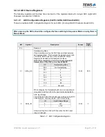
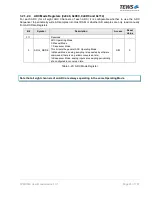
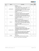
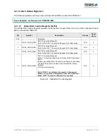
3.2.1.3.1
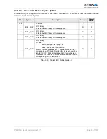
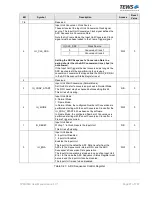
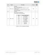
ADC Sequencer Control Register (0x120)
Bit
Symbol
Description
Access
Reset
Value
31:19
-
Reserved
-
-
18
DMA_STAT_ENA
DMA Status Transfer Enable
0: DMA Status Transfer Disabled
1: DMA Status Transfer Enabled
If enabled, after a DMA Buffer termination event, the DMA
Status is transferred to the Host RAM location configured in
the DMA Status Base Address Register.
R/W
0
17
WR_DMA_RESET
DMA Reset
Writing '1' to this bit resets the DMA Controller.
This bit is self-clearing
R/S
0
16
WR_DMA_ENA
DMA Enable
0: DMA Controller Disabled
1: DMA Controller Enabled
Enables the Sequencer's DMA Controller to allow the
initiation of DMA transfers by writing to the DMA Buffer
Length Register.
When being disabled, any active DMA transfer is completed
before the DMA Engine enters Idle or Error state.
The DMA Controller operation is stopped in case of a DMA
Error. In this case the DAC Sequencer Status Register must
be read and the DMA Controller can be disabled.
The DMA Controller is reset when disabled.
R/W
0
15:9
-
Reserved
-
-
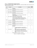
8
ADC_SEQ_FIFO_CLR
FIFO Clear
When set to 1, the ADC Sequencer's internal FIFO is
cleared.
This bit is self-clearing
R/S
0

