


TPCE636 User Manual Issue 1.0.2
Page 67 of 104
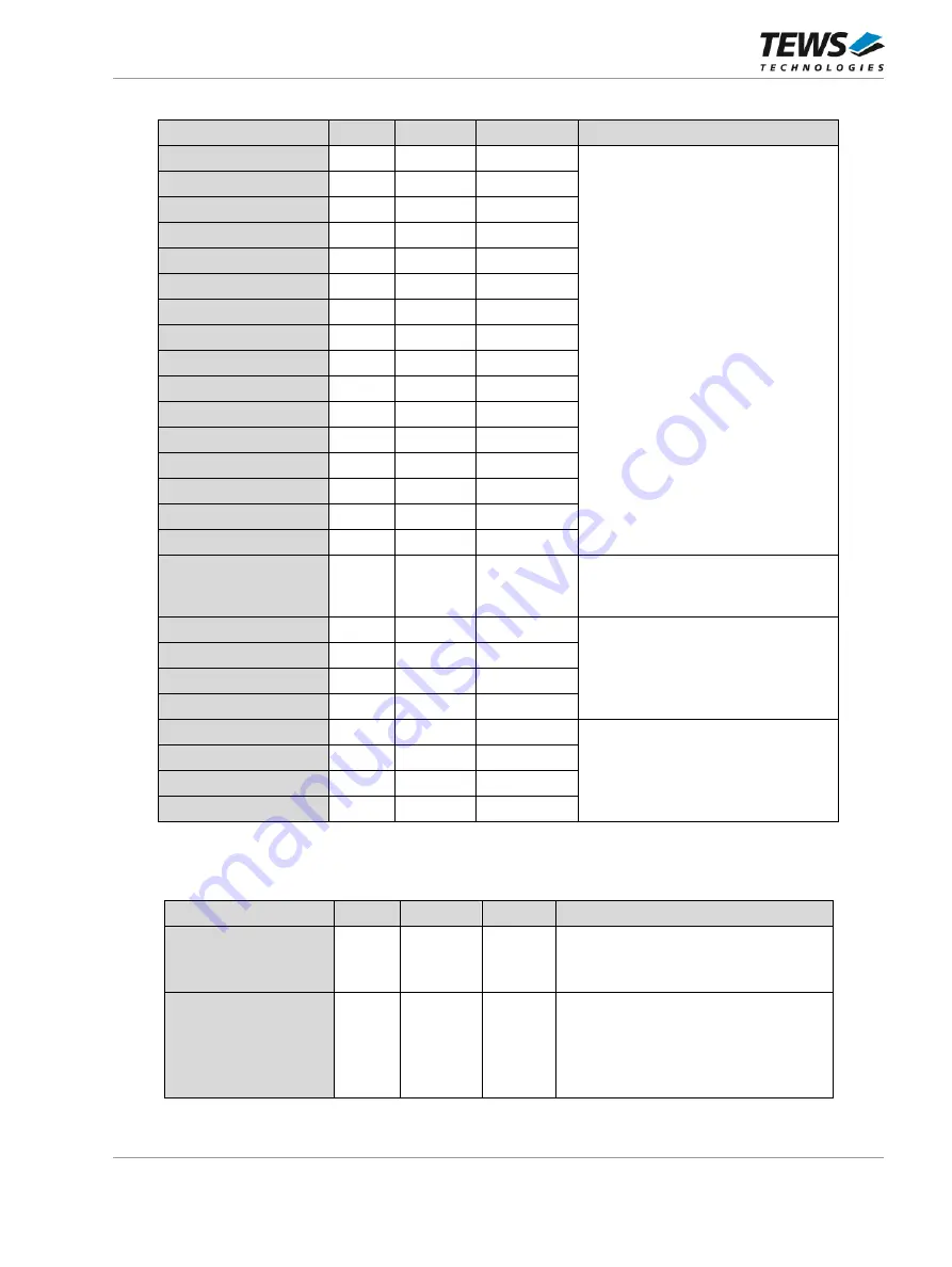
Second DAC configuration interface is for controlling the DAC channel 8 up to 15.
Signal
Bank
VCCO
Pin
Description
DAC_D16
15
3.3V
G15
Second DAC Data Bus to
DAC Device 4 .. 7
with
DAC Channel 8 .. 15
DAC_D17
15
3.3V
H18
DAC_D18
15
3.3V
K15
DAC_D19
15
3.3V
K20
DAC_D20
15
3.3V
J18
DAC_D21
15
3.3V
J19
DAC_D22
15
3.3V
J20
DAC_D23
15
3.3V
A19
DAC_D24
15
3.3V
B17
DAC_D25
15
3.3V
C17
DAC_D26
15
3.3V
L20
DAC_D27
15
3.3V
H16
DAC_D28
15
3.3V
G20
DAC_D29
15
3.3V
A18
DAC_D30
15
3.3V
G17
DAC_D31
15
3.3V
D18
DAC_ADR1
15
3.3V
G19
DAC Address Line to select the
DAC channel A or B from one
DAC Device.
DAC_'WR08_09'
15
3.3V
L19
A low active WR transfers data to
DAC input register.
One write signal for each DAC
device respectively for two DAC
channel.
DAC_'WR10_11'
15
3.3V
H19
DAC_'WR12_13'
15
3.3V
K16
DAC_'WR14_15'
15
3.3V
K17
DAC_LDAC08_09
14
3.3V
H24
Load the DAC output register with
contents of the input register.
One write signal for each DAC
device respectively for two DAC
channel.
DAC_LDAC10_11
14
3.3V
J21
DAC_LDAC12_13
14
3.3V
H22
DAC_LDAC14_15
14
3.3V
J24
The following signals are used for all 16 DAC channels.
Signal
Bank
VCCO
Pin
Description
DAC_RS#
12
2.5V
W25
Active low resets all 16 input and
output DAC registers.
Value depends on DAC_MSB line.
DAC_MSB
12
2.5V
W26
MSB Power-On Reset State.
DAC_MSB = 0 corresponds to zero-
scale reset;
DAC_MSB = 1 corresponds to
midscale reset
Table 7-17: TPCE636 parallel DAC Interface


