Teledyne ADQ8-4X Скачать руководство пользователя страница 6

19-2302 A 
2020-09-16

6(46)

ADQ8-4X Manual

19-2302 A 2020-09-16

6(46)

The number representation is 2’s complement. The full scale maximum code is then 32 704 and the full 
scale minimum code is –32 768. Overflow or underflow at any position in the signal path will saturate 
the data and turn on an overflow flag. See 

Section 7.10

 for more information on over- and under-flow. 

1.2.2

Calibration

During the factory calibration procedure the analog properties are measured and parameters for a digi-
tal compensation are computed. An analog deviation in the front-end is thus compensated for by the 
inverse function in the digital signal processing part. 

Example 1: With the variable gain –VG option (always included with the ADQ8-4X), the user requests 
a range. The closest available setting is selected and the actual range is returned to the user for being 
used in the user’s algorithms, see 

Section 2.1

Example 2: The full scale signal range of the ADQ is measured in production and the 

SetGainAndOff-

set

 function is used for adjusting to the correct signal range. 

1.2.3

Data acquisition nomenclature 

Table 1

 defines some key data acquisition terms. 

1.2.4

Sampling clock frequency

The ADQ8-4X is designed for the specified 2 GHz clock frequency only with the firmware FWDAQ. The 
firmware FW4GDAQ enables sampling at 4 GSPS. A different sampling rate can be achieved by using 
the sample skip function

Section 5.10

.

1.2.5

System clocks 

The different parts of the digitizer operate on different clock rates
The sampling of the analog signal is done on the sampling clock of the ADC (see 

Section 1.2.4

). 

The external trigger input has a trigger clock which is higher than or equal to the sampling clock for high 
trigger time precision (4 GHz). This clock frequency is the same regardless of selected sampling fre-
quency. 
The PCIe host PC connections has its own clock system. 

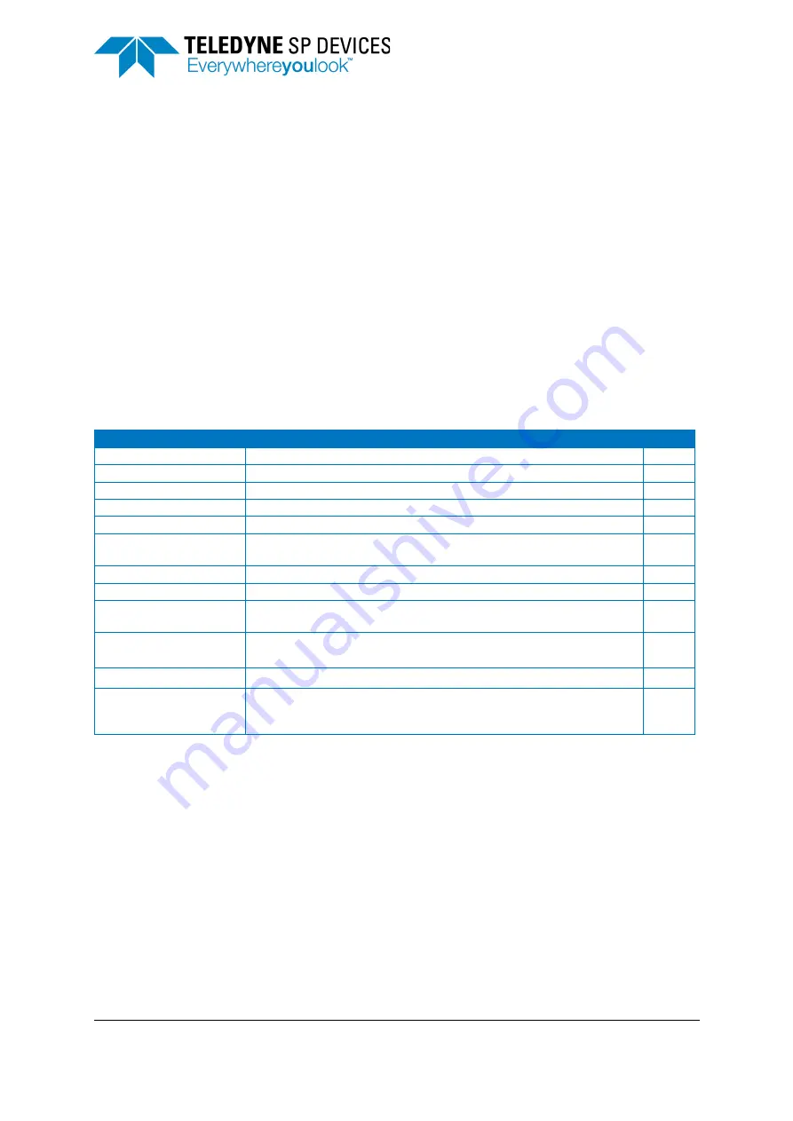
Table 1:   Data recording nomenclature. 

PARAMETER

DESCRIPTION

REF

ADQ

Collective name for digitizers from Teledyne SP Devices.

Analog

Analog signal is the input to the digitizer. This is the signal to be digitized. 

Waveform

Analog signal with a distribution in time. This is digitized into a record. 

Sample

An analog signal level is digitized into a sample, that is a numerical value. 

SYNC

Physical connector on the front panel.

4.8

6.1

Record

A set of consecutive samples is called a record. An analog waveform is 
digitized into a record of samples. 

4

TRIG

Physical connector on the front panel.

4.8

6.1

Trigger

Trigger is an event that starts acquisition of a record. 

4.3

Timestamp

Timestamp is a real-time value that identifies when a trigger happened. 
The timestamp gives timing information for each sample. 

4.4

GSPS

Giga-samples per second (10

9

). Clock frequency [Hz] and sample rate 

[SPS] are both used to denote speed. 

MSPS

Mega-sample per second (10

6

). 

DC-offset

This is an analog DC level which is added to the analog input signal inside 
the digitizer to vertically move the analog signal to fit within the range of 
the digitizer. This effectively doubles the ENOB for a unipolar signal. 

2

Содержание ADQ8-4X

Страница 1: ...com Regional sales offices www spdevices com contact Manual ADQ8 4X This manual describes how to get the full potential out of Teledyne SP Devices digitizer ADQ8 4X The manual includes these steps Set up the analog front end Master the triggers Control the acquisition Manage the sampling clock Understanding data transfer to host PC Using GPIO ...

Страница 2: ...definitions 14 4 4 2 Timestamp reset 14 4 5 Blocking triggers for synchronization 16 4 5 1 Function overview 16 4 5 2 Block triggers once 18 4 5 3 Windowing triggers 18 4 5 4 Gating and windowing triggers 18 4 5 5 Programming sequence for using trigger blocking 18 4 6 Trigger jitter 19 4 6 1 Trigger jitter definitions 19 4 6 2 Asynchronous triggering 19 4 6 3 Synchronous trigger 20 4 6 4 Extended ...

Страница 3: ...33 6 2 ADQ8 4X PXIe GPIO on SYNC connectors 34 6 3 Using GPIO as a trigger 34 6 4 Output 34 6 5 GPIO in ADQ Development Kit 34 7 ACQUISITION CONTROL 35 7 1 Multi thread notice 35 7 2 Acquisition memory 35 7 3 Triggered streaming acquisition 36 7 4 Acquisition mode multi record 36 7 5 Re arm time 37 7 6 User scheduled data transfer mode 38 7 6 1 Transfer buffers 40 7 6 2 User s buffers 40 7 7 Strea...

Страница 4: ...19 2302 A 2020 09 16 4 46 ADQ8 4X Manual 19 2302 A 2020 09 16 4 46 9 REFERENCES 45 ...

Страница 5: ...uing 1 2 1 Data format The ADC components of ADQ8 4X has 10 bits resolution while the data format inside the ADQ8 4X and out to the host PC is 16 bits The 16 bits from the ADCs are MSB aligned in this 16 bit data word Thus the 6 LSBs are zero DESCRIPTION REFERENCE a Signal conditioning analog front end 2 b High speed and high resolution A D converters 3 c Calibration of gain and offset 2 d Teledyn...

Страница 6: ...clocks The different parts of the digitizer operate on different clock rates The sampling of the analog signal is done on the sampling clock of the ADC see Section 1 2 4 The external trigger input has a trigger clock which is higher than or equal to the sampling clock for high trigger time precision 4 GHz This clock frequency is the same regardless of selected sampling fre quency The PCIe host PC ...

Страница 7: ...n the gain setting With for example a range of 500 mVpp the ana log input signal can vary from 250 mV to 250 mV and the range can be moved from 0 mV 500 mV to 500 mV 0 mV by the DC offset feature Section 2 3 The maximum digital code 2 15 represents an analog signal with a level ACTUAL_ANALOG_RANGE 2 at the input A specific analog signal ANALOG_LEVEL will then be represented by the following digita...

Страница 8: ...io These blocks are linked as in Figure 2 Digitizer Studio is described in 5 BLOCK DESCRIPTION REF a Analog front end Setting up analog input parameters digital signal transformation 2 b DBS Digital Baseline Stabilizer signal conditioning IP 3 c Acquisition control Setting up the recording of data 7 d Transfer to PC Data transfer methods to move the data to the PC 8 e Trigger Trigger synchronizati...

Страница 9: ...code DIGITAL_CODE_LEVEL ANALOG_LEVEL ACTUAL_ANALOG_RANGE 2 2 15 3 DESCRIPTION USER COMMAND REF a The analog input impedance 50 to GND b On ADQ8 4X VG the gain can be set in a discrete number of steps By requesting a certain range the closest available setting is activated The actual range that is set is returned to the user Note that the compensation has to be done in the software Changing the inp...

Страница 10: ...of the DC offset generator the actual digital codes read out from the ADQ may differ from the expected level For accurate baseline measurements the Digital Baseline Stabilizer DBS offers a digital correction of the baseline to an accuracy of 22 bits Section 3 1 2 4 Adjusting the digital gain and offset The digital gain and offset block is primarily intended for factory calibration but it may also ...

Страница 11: ...cally locks the baseline to a user defined value Note that DBS is off at power up DBS has to be activated by the user s application software The time when DBS is activated is important To get a good initial estimate DBS should be activated when there is very little signal energy present at the input If there is too much signal power in the initial estimate the convergence of DBS is slowed down Not...

Страница 12: ...gger input on front panel connector SYNC 4 8 2 h Select which type of trigger to activate SetTriggerMode i The trigger blocking function controls the flow of triggers to the acquisition engine SetupTriggerBlocking 4 5 j Select which channels to record data from MultirecordSetChannelMask k Acquisition engine creates a record from streaming data 7 l Records are sent to data FIFO for transfer to the ...

Страница 13: ...e data record is controlled by the parameters pretrigger and trigger delay The pretrigger buffer enables capturing data prior to the trigger event Figure 5 Use the command Set PreTrigSamples to define the pretrigger The trigger delay postpone the start of the acquisition of the data record specified number of samples after the trigger event Figure 6 Use the command SetTriggerHoldOffSamples to defi...

Страница 14: ... timestamp counter also free run ning See Section 5 for all details about the clock system of digitizer The timestamp counter measures the time from a reference time point to the trigger event The refer ence time point is when the counter is started or reset See Section 4 4 2 for information on how to reset the timestamp counter Example 3 Assume an ADQ8 4X sampling with a clock frequency at 2 GSPS...

Страница 15: ...AMP TIME_STAMP_OF_RECORD TIME_STAMP_REFERENCE 3 The third method is to apply an external trigger to reset the timestamp reset Figure 7 This method has the possibility to synchronize several boards to full precision of the external trigger See Sec tion 4 5 The sequence of operation is DisarmTimestampSync SetupTimestampSync ArmTimestampSync The number of reset pulses are counted and the information ...

Страница 16: ...g ger blocking and the timestamp reset the timestamp is aligned to the start of the acquisition The trig ger blocker source can be most available trigger sources Figure 8 a b c Note the order of the commands for activating triggers and trigger blockers Figure 8 e g h i DESCRIPTION USER COMMAND REF a External trigger input signal on front panel connector 4 8 b External sync input signal on front pa...

Страница 17: ...g f This signal is ignored as the trigger blocker is not armed g Select trigger source SetTriggerMode h Start receiving triggers Note that triggers are still blocked ArmTrigger i The unblocking of triggers is armed and can be activated by d ArmTriggerBlocking j Triggers are blocked until the first accepted blocker signal SetupTriggerBlocking 4 5 k The trigger blocker can also be set up with a wind...

Страница 18: ...r signal is a point trigger and a sync signal is a line trigger 4 5 4 Gating and windowing triggers The gate mode for blocking triggers is illustrated in Figure 8 l The length of the window where trig gers are accepted is equal to the length of the trigger blocking signal 4 5 5 Programming sequence for using trigger blocking The order of commands is important when programming the trigger blocking ...

Страница 19: ... The RMS value of such a process is TRIGGER_CLOCK_PERIOD sqrt 12 The highest resolution is achieved with an external trigger connected to the TRIG connector ADQ8 4X has a trigger clock at 4 GSPS TRIGGER_CLOCK_PERIOD of 250 ps and a trigger jitter of 72 ps RMS theoretical value Section 4 6 4 See Table 2 for time resolution all the external trigger sources 4 6 2 Asynchronous triggering If the trigge...

Страница 20: ...the timestamp information Section 4 4 The position of the first sample is rounded up from the trigger position The parameter RECORD_START tells where the trigger was Referring to Figure 11 the RECORD_START parameter can have values in the range 250 ps up to 500 ps A positive value means that the first sample is after the trigger The given range is without pretrigger or trigger delay With pretrigge...

Страница 21: ...he trigger edge to rising or falling to adjust to the polarity of the trigger signal CONNECTOR DESCRIPTION TIME RESOLUTION TOTAL JITTER IMPEDANCE TRIG LEVEL REF TRIG External trigger on front panel 250 ps 76 ps 50 500 SW contr 4 8 1 SYNC Sync signal on front panel 4 ns 1 2 ns 50 500 1 1 500 option available on MTCA form factor only SW contr 4 8 2 STARB Backplane trigger in PXIe systems Requires tr...

Страница 22: ...nse and low reflections which is important for precise timing However in a high fan out situation where a trigger source has to drive many nodes the load can be too high The trigger input can then be set in a high impedance mode and a bussed connection can be used Figure 14 In Figure 14 a an external source is driving the array of ADQ digitizers In Figure 14 b one of the ADQ digitizer is used as a...

Страница 23: ...ger lines from the system timing slot To use these triggers a dedicated timing generation board has to be used in the system timing slot The TRIG bus is a general bus in the backplane which can be used for triggering The digitizer support connection to port 0 and port 1 of that bus The backplane trigger support both input and output triggers These operations are independent and can be used simulta...

Страница 24: ...ESCRIPTION USER COMMAND REF a Backplane Trigger bus and DSTAR connections b Set direction for each port in the backplane SetDirectionPXI c Output Select output port for trigger output signal SetupTriggerOutput 4 12 d Output This is the source for the trigger output signal SetupTriggerOutput 4 12 e Input Select port for trigger sources SetTriggerMaskPXI f Input The backplane trigger signal is OR ed...

Страница 25: ... ACTUAL_ANALOG_RANGE 2 2 15 12 4 10 3 Controlling noise sensitivity The level trigger is sensitive to noise since it can detect a step as small as one digital code This can cause unwanted triggering The noise sensitivity is controlled by a hysteresis function Figure 17 After triggering the signal has to cross a reset level before it can trigger again Setting the reset level far from the trigger le...

Страница 26: ...er output signal Note that the trigger output is the same physical TRIG connector as the external trigger input 4 12 1 Trigger output port selection The trigger output port is selected to one of these ports Trigger connector on the front panel Note that the trigger output is the same physical TRIG con nector as the external trigger input PXIe backplane triggers Section 4 9 1 4 12 2 Frame sync outp...

Страница 27: ...igitizer The trigger ing is then done inside the FPGA as a logical signal and the trigger time is guaranteed to be exact on the expected sample The external connection is preferred when the trigger is used for triggering both the digitizer and the external equipment Then the ADQ will listen to the same physical signal as the external equipment is using DESCRIPTION USER COMMAND REF a Internal trigg...

Страница 28: ...ers in the system 4 13 3 High precision trigger on analog input The source for the trigger can be any available trigger If one of the analog inputs is used as a high pre cision input the trigger timing can be computed to 25 ps trigger precision 4 13 4 Calibration To reach the trigger accuracy of 200 ps for the entire chassis installation the system has to be cali brated in the factory 5 DESCRIPTIO...

Страница 29: ...source in the primary unit This may be an analog channel using level trigger or any other trigger source DaisyChainSetTriggerSource DaisyChainSetupLevelTrigger c The trigger signal is synchronized to the clock reference and forwarded to the secondary units This daisy chain of triggers can include many cards DaisyChainSetupOutput DaisyChainEnableOutput d The data is triggered on the synchronized tr...

Страница 30: ...parallel to maintain the throughput The Data Clock is also synchronized to the clock reference Finally the host PC interface also operate on a different clock The PCIe system clock is provided from the PCIe bus This part of the design is not phase locked to the sampling clock 5 2 Flexible clock network The preferred clock method is a systems design parameter and teh digitizer supports many options...

Страница 31: ...parts of the system may be necessary To support that the ADQ offers several options to accept an external clock refer ence A long term phase stability to other equipment is then guaranteed DESCRIPTION USER COMMAND REF a The input SMA connector is common for external clock reference input external clock input The impedance is 50 SetClockSource 5 3 b The output MCX connector drives the selected cloc...

Страница 32: ... 5 8 External clock If the system is designed with an external high quality signal it may be used for clocking the ADQ If an external clock source is used all the internal clocks are generated from that to maintain the phase and frequency ratio 5 9 Clock reference output In addition to the synchronization solution with an external clock reference source the digitizer can also act as master and out...

Страница 33: ...d in the block dia gram in Figure 23 DESCRIPTION USER COMMAND REF a The external pin is automatically connected to the activated function 6 3 b The GPIO input function always reads the state of the pin The GPIO output function is activated by the user SetDirectionGPIOPort 6 3 6 4 c The user may access the pin by reading and writing from the software ReadGPIOPort WriteGPIOPort 6 3 6 4 d The user ma...

Страница 34: ...RIG connector 4 ArmTrigger 5 WriteGPIOPort 1 This sends a signal on the TRIG connector that triggers the devices The GPIO input function always listen to the trigger pin This means that the external trigger pin value can always be read from the GPIO function ReadGPIOPort 6 4 Output The output is activated through the software command SetDirectionGPIOPort and the signal level is set by WriteGPIOPor...

Страница 35: ...ly one channel is activated the entire memory is available for that channel The data memory is also shared between data and headers Table 3 A header contains information about the data record for example timestamp and channel number The headers can be setup in two different modes In the normal mode the headers are activated This mode is recommended for all standard acqui sition modes In the raw mo...

Страница 36: ...buffer can hold one record Data is then written constantly into this buffer until the trigger event arrives After the trigger event Record_length Pretrigger_samples is written into the buffer The accumulation of the record is then completed The circular buffer contains the pre trigger data and the post trigger data The position of the trigger may be anywhere in the buffer The API unwraps the data ...

Страница 37: ... the digitizer prepares the DRAM for receiving the next record The re arm time is thus a hardware related fixed timing during which the digitizer cannot record The scheduling of triggers depends on the re arm time but also of the pre tirgger and the trigger delay See Figure 29 for an illustration of the timing relation between trigger and acquisition Figure 27 Multi record organization of memory F...

Страница 38: ...sition and after that requests the data This is the straight forward method if the total amount of data is less than the data buffer size Section 7 2 that is it can be stored in the buffer of the digitizer Note that if using readout while recording the multi record is not automatically limited by the data buffer size A block diagram of triggered streaming acquisition and user scheduled data transf...

Страница 39: ...IFO on the ADQ d The DMA transfers data to the PC when requested by the user e Kernel buffers in the host PC receives the data from the digitizer f The ADQAPI receives incoming data and do necessary pre processing for example lost packages and sends data to the user s buffers g User s buffers in RAM These are accessed via API commands h The user s application sets up the digitizer for acquiring da...

Страница 40: ...of buffers one for header information and one for data The header is always 40 bytes per record and the content is described in Section 7 9 The data buffer size is depending on the amount of data in each record For FWDAQ the record size is always constant and the buffer size can be set to match the record size The example code in ADQAPI_example1 illustrate how to handle data buffers in general 7 7...

Страница 41: ...itional information about e g the experiment is added to the header c Header and data is analyzed in real time and only requested parameters are stored 7 9 Figure 32 Data flow through the system PARAMETER FORMAT DESCRIPTION REF Record Status Byte Over under range FIFO fill factor and lost data 7 9 2 User ID Byte A user configurable value to identify the ADQ unit 7 9 3 Channel Byte The channel numb...

Страница 42: ...combinations are available for ADQ Development Kit users to create artificial channels 7 9 6 Record number The Record number is counting the number of records captured from the power up of the digitizer 7 9 7 Data format The header data parameter Data format Table 4 informs the user on how to interpret data Allowed values are given in Table 6 7 9 8 Record length This is the length of the data reco...

Страница 43: ...h offset b Digital offset calibration c Digital baseline stabilizer that dynamically adjust baseline to zero That is adjust the offset Under range has already occurred prior to this stage d Acquisition create a header which contain over under range indication e The analog input signal with offset The ADC also contribute to the offset f Digital calibration cannot account for offset on the analog si...

Страница 44: ...ach software command contains a pointer to the control unit for all ADQ digitizers and an instance number that points out the current ADQ To identify a specific unit read the serial number GetBoardSerialNumber This gives a mapping between the instance number and a physical unit The record header Table 4 contains a byte field User ID where the user can set an identifier for each card This gives a m...

Страница 45: ... 16 45 46 9 REFERENCES 1 17 1998 ADQ8 4X Datasheet 2 14 1351 ADQAPI Reference guide 3 08 0214 ADQAPI User guide 4 18 2059 ADQUpdater user guide 5 20 2382 Digitizer Studio manual 6 19 2246 ADQ8 Daisy Chain Board synchronization 7 20 2465 ADQ8 Triggered streaming ...

Страница 46: ...entities other than Teledyne SP Devices The warranty of replacement products shall terminate with the warranty of the product Buyer shall not return any products for any reason without the prior written authorization of Teledyne SP Devices In no event shall Teledyne SP Devices be liable for any damages arising out of or related to this docu ment or the information contained in it TELEDYNE SP DEVIC...

Отзывы: