background image

Chapter 2: Installation

2-9

2-7 Connector 

Defi nitions 

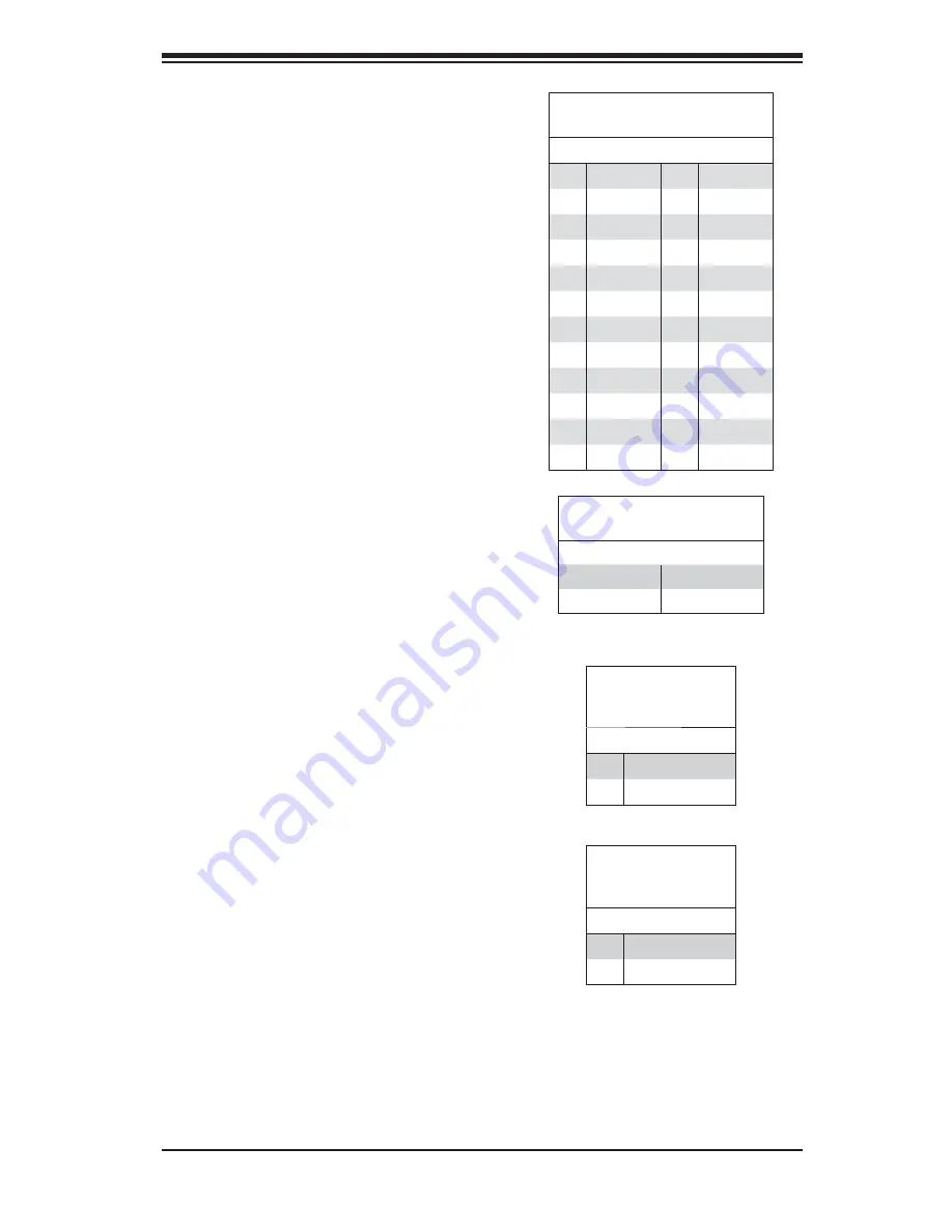
Power Connectors 

 A 24-pin main power supply connector(JPW1) 

and two 8-pin CPU PWR connectors 

(JPW2/JPW3) on the motherboard. These 

power connectors meet the SSI EPS 12V 

specifi cation. In addition to the 24-pin ATX 

power connector, the 12V 8-pin CPU PWR 

connector at JPW2 and JPW3 must also be 

connected to your power supply. See the 

table on the right for pin defi nitions. 

Warning

: To prevent damage to the power 

supply or motherboard, please use a power 

supply that contains both a 24-pin and 8-pin 

power connectors. Be sure to connect these 

connectors to the 24-pin (JPW1) and the two 

8-pin (JPW2/JPW3) power connectors on the 

motherboard. Failure in doing so will void the 

manufacturer warranty on your power supply 

and motherboard.

ATX Power 24-pin Connector

Pin Defi nitions

Pin#   Defi nition       Pin #   Defi nition

13

+3.3V

1

+3.3V

14

-12V

2

+3.3V

15

COM

3

COM

16

PS_ON

4

+5V

17

COM

5

COM

18

COM

6

+5V

19

COM

7

COM

20

Res (NC)

8

PWR_OK

21

+5V

9

5VSB

22

+5V

10

+12V

23

+5V

11

+12V

24

COM

12

+3.3V

Required Connection

12V 8-pin  PWR Connector

Pin Defi nitions

Pins                      Defi nition

1 through 4

Ground

5 through 8

+12V

Power LED Connector

The Power LED connector is on pins 15 and 

16 of JF1. This header should be connected 

to the chassis power LED connection. See 

the table on the right for pin defi nitions.

Power LED

Pin Defi nitions 

(JF1)

Pin#   Defi nition

15

3.3V

16

Power LED

HDD/FP UID Switch

The HDD/UID Switch connections are 

located on pins 13/14 of JF1. Attach a 

hard-drive LED cable to display HDD or 

SATA activities. This connection can also 

be used as a front panel UID (Unit Identifi  

er) switch. The UID LED on Pin 7 of JF1 

works in conjunction with this UID Switch. 

When the user presses and releases the UID 

switch, the UID LED will be turned on or off 

to indicate the location of the unit. (Refer to 

Page 2-11 for more details.)

HDD/UID Switch

Pin Defi  nitions 

(JF1)

Pin#   Defi nition

13

UID Signal/3.3V

14

HDD Active

Содержание H8DG6

Страница 1: ...H8DGi H8DGi F H8DG6 H8DG6 F USER S MANUAL Revision 1 1b SUPER...

Страница 2: ...of any such disputes Super Micro s total liability for all claims will not exceed the price paid for the hardware product FCC Statement This equipment has been tested and found to comply with the limi...

Страница 3: ...rboard box describes the features specifications and performance of the motherboard and provides detailed information about the chipset Chapter 2 begins with instructions on handling static sensitive...

Страница 4: ...iv H8DG6 i F Serverboard User s Manual Notes...

Страница 5: ...ons 2 1 Unpacking 2 1 2 2 Processor and Heatsink Installation 2 2 2 3 Mounting the Motherboard into a Chassis 2 4 2 4 Installing Memory 2 4 DIMM Module Population Configuration 2 6 2 5 PCI Expansion C...

Страница 6: ...2 15 2 8 Jumper Settings 2 16 Explanation of Jumpers 2 16 CMOS Clear 2 16 LAN Enable Disable 2 17 SAS Enable Disable 2 17 VGA Enable Disable 2 17 I2C to PCI Express Slot 2 17 BMC Jumper 2 17 Watch Dog...

Страница 7: ...cedures 3 1 Before Power On 3 1 No Power 3 1 No Video 3 2 Memory Errors 3 2 Losing the System s Setup Configuration 3 2 3 2 Technical Support Procedures 3 3 3 3 Frequently Asked Questions 3 3 3 4 Retu...

Страница 8: ...Notes viii H8DG6 i F Serverboard User s Manual...

Страница 9: ...ance Please check that the following items have all been included with your motherboard If anything listed here is damaged or missing contact your retailer One 1 H8DG6 i F serverboard One 1 I O shield...

Страница 10: ...ope Address Super Micro Computer B V Het Sterrenbeeld 28 5215 ML s Hertogenbosch The Netherlands Tel 31 0 73 6400390 Fax 31 0 73 6416525 Email sales supermicro nl General Information support supermicr...

Страница 11: ...Chapter 1 Introduction 1 3 Figure 1 1 H8DG6 i F Image...

Страница 12: ...3 FAN2 FAN5 FAN7 CPU1 FAN1 FAN6 FAN8 CPU2 JPI2C1 SAS 4 7 JPW1 JPW3 JPW2 BMC Windbond COM1 SLOT6 PCI E 2 0 X16 SLOT5 PCI E 2 0 X4 IN X8 COM2 USB7 USB6 USB2 3 USB4 5 SATA0 SATA1 SATA2 SATA3 SATA4 SATA5...

Страница 13: ...abled JPG1 VGA Enable Disable Pins 1 2 Enabled JPL1 LAN 1 Enable Disable Pins 1 2 Enabled JPS1 SAS Controller Enable Disable Pins 1 2 Enabled JWD1 Watch Dog Pins 1 2 Reset LED Description LAN Ports LE...

Страница 14: ...ower I2 C Header JPW1 24 pin Main ATX Power Connector JPW2 3 12V 8 pin CPU Power Connectors JTPM1 Trusted Platform Module Header JSMB1 System Management Bus Header SMBus JWF1 SATA DOM Disk_On_Module P...

Страница 15: ...bridge chipset Expansion Slots Three 3 PCI Express x16 Gen 2 One 1 PCI Express x8 Gen 2 Two 2 PCI Express x4 in x8 slot Gen 2 BIOS 16 Mb AMIBIOS SPI Flash ROM DMI 2 3 PCI 2 2 ACPI 1 0 ACPI 2 0 is BIOS...

Страница 16: ...Eight 8 USB Universal Serial Bus 2 0 ports 2x rear 2x headers USB 2 3 and USB 4 5 2x type A Two 2 LAN ports supported by one onboard Intel 82576 Ethernet controllers for 10 100 1000Base T One 1 dedica...

Страница 17: ...16 x16 bits 6 4GHz USB USB PORT X8 LSI SAS2 2008 PCIE X8 LAN Intel 82576 PCIE x4 AMD SP5100 Winbond WPCM450 VGA HT Link AMD SR5690 2 16 16 2 6GHz DDR3 1600 1333 1066 PCIE X4 SLOT 5 PCIE_ X4 G34 SOCKET...

Страница 18: ...48x between integrated circuits This is done partly by reducing the number of buses in the chipset to reduce bottlenecks and by enabling a more efficient use of memory in multi processor systems The...

Страница 19: ...cribes the features of your motherboard that deal with power and power settings Microsoft OnNow The OnNow design initiative is a comprehensive system wide approach to system and device power control O...

Страница 20: ...occur after hours and on weekends so that daily LAN traffic is kept to a minimum and users are not interrupted The motherboard has a 3 pin header WOL to connect to the 3 pin header on a Network Interf...

Страница 21: ...ommunication Each UART includes a 16 byte send receive FIFO a programmable baud rate generator complete modem control capability and a processor interrupt system Both UARTs provide legacy speed with b...

Страница 22: ...1 14 H8DG6 i F Serverboard User s Manual Notes...

Страница 23: ...its components peripheral chips memory modules or gold contacts When handling chips or modules avoid touching their pins Put the motherboard and peripherals back into their antistatic bags when not i...

Страница 24: ...Procedure Follow the procedures as listed below to install the motherboard into a chassis 1 Install the processor s and the heatsink s 2 Install the motherboard in the chassis 3 Install the memory and...

Страница 25: ...e CPU horizontally or vertically or rub the CPU against the socket or against any pins of the socket which may damage the CPU and or the socket 5 With the CPU inserted into the socket inspect the four...

Страница 26: ...nto the Tray in the Chassis 1 Carefully mount the motherboard onto the motherboard tray by aligning the motherboard mounting holes with the raised metal standoffs in the tray 2 Insert screws into all...

Страница 27: ...00 1333 1066 registered ECC Unbuffered ECC non ECC SDRAM Populating two adjacent slots at a time with memory modules of the same size and type will result in interleaved 128 bit memory which is faster...

Страница 28: ...3B P2 4A P2 4B DIMM Module Population Configuration For memory to work properly follow the tables below for memory installation Per Channel DIMM Populations Options DIMM Type DIMM A DIMM B Max MHz 1 5...

Страница 29: ...assis remove the PCI slot shield 7 Slide the add on card into the riser card and attach the add on card bracket in place of the PCI slot shield 8 Secure the add on card by closing the PCI slot shield...

Страница 30: ...r various front control panel connectors See Figure 2 3 for the pin definitions of the various connectors Refer to Section 2 6 for details Figure 2 3 JF1 Front Control Panel Header JF1 Power Button 2...

Страница 31: ...3V 14 12V 2 3 3V 15 COM 3 COM 16 PS_ON 4 5V 17 COM 5 COM 18 COM 6 5V 19 COM 7 COM 20 Res NC 8 PWR_OK 21 5V 9 5VSB 22 5V 10 12V 23 5V 11 12V 24 COM 12 3 3V Required Connection 12V 8 pin PWR Connector P...

Страница 32: ...Refer to the table on the right for pin definitions OH Fan Fail PWR Fail Blue_UID LEDPin Defi nitions JF1 Pin Definition 7 Blue_LED Cathode UID 5 5V SB 8 OH Fan Fail PWR Fail UID LED Red OH Fan Fail...

Страница 33: ...tions COM1 COM2 Pin Definition Pin Definition 1 DCD 6 DSR 2 RXD 7 RTS 3 TXD 8 CTS 4 DTR 9 RI 5 Ground 10 NC Power LED Speaker On the JD1 header pins 1 3 are used for power LED indication and pins 4 7...

Страница 34: ...ted Platform Module TPM available separately from a third party vendor A TPM is a security device that allows encryption and authentica tion of hard drives disallowing access if the TPM associated wit...

Страница 35: ...ctor for SATA DOM Disk_ On_Module is located at JWF1 Connect the appropriate cable here to provide power support for your DOM devices Wake On LAN The Wake On LAN header is designated JWOL1 See the tab...

Страница 36: ...7 USB0 Pin Definition USB1 Pin Definition 1 5V 1 5V 2 PO 2 PO 3 PO 3 PO 4 Ground 4 Ground USB Headers Four USB 2 0 headers USB2 3 and USB4 5 are also included on the motherboard These may be connected...

Страница 37: ...VGA connector is located below the COM Port on the IO backplane This connector is used to provide video and CRT display JIBTN1 Header only on H8DG6 F A RAIDKey header located at JIBTN1 provides RAID...

Страница 38: ...he jumper is on and Open means the jumper is off the pins Connector Pins Jumper Setting 3 2 1 3 2 1 CMOS Clear JBT1 is used to clear CMOS which will also clear any passwords Instead of pins this jumpe...

Страница 39: ...settings BMC Jumper Enable JPB1 Jumper Settings Jumper Setting Definition Pins 1 2 Enabled default Pins 2 3 Disabled VGA Enable Disable JPG1 allows you to enable or disable the VGA port The default p...

Страница 40: ...enabled in BIOS Note When Watch Dog is enabled the user must write their own application software to disable the Watch Dog Timer Watch Dog Jumper Settings JWD1 Jumper Setting Definition Pins 1 2 Rese...

Страница 41: ...The LEDS1 SAS2008 Heartbeat LED shows SAS2 activity on the serverboard See the table to the right for information on this LED BMC Heartbeat DP1 LED Settings Color Status Definition Green Blinking BMC...

Страница 42: ...initions SATA Ports Pin Definitions SATA0 SATA5 Pin Definition 1 Ground 2 TXP 3 TXN 4 Ground 5 RXN 6 RXP 7 Ground SAS Ports Pin Definitions SAS0 SAS7 Pin Definition Pin Definition 1 Ground 2 TXP 3 TXN...

Страница 43: ...alling the OS operating system and SATA RAID driver you must decide if you wish to have the operating system installed as part of a bootable RAID array or installed to a separate non RAID hard drive I...

Страница 44: ...d hit the Del key to enter the BIOS Setup Utlility After the Setup Utility loads 1 Use the arrow keys to move to the Exit menu Scroll down with the arrow keys to the Load Optimal Defaults setting and...

Страница 45: ...ing the RAID Driver During OS Installation You may also use the procedure below to install the RAID driver during the Window s OS installation 1 With the Windows OS installation CD in the CD ROM drive...

Страница 46: ...he icon representing your CD ROM drive Finally double click on the S Setup icon Click the icons showing a hand writing on paper to view the readme files for each item Click the computer icons to the r...

Страница 47: ...m information such as CPU temperature system voltages and fan status See the Figure below for a display of the SuperDoctor III interface Note The default User Name and Password for SuperDoctor III is...

Страница 48: ...er s Manual can be downloaded from the Supermicro web site at http www supermicro com products accessories software SuperDoctorIII cfm For Linux we recommend that you use the SuperoDoctor II applicati...

Страница 49: ...ur power supply 3 Make sure that no short circuits exist between the motherboard and chassis 4 Disconnect all cables from the motherboard including those for the keyboard and mouse 5 Remove all add on...

Страница 50: ...talled 2 You should be using proper ECC DDR 3 memory see next page Also it is recommended that you use the same memory type and speed for all DIMMs in the system See Section 2 4 for memory details 3 C...

Страница 51: ...PCB revision number BIOS release date version this can be seen on the initial display when your system first boots up System configuration An example of a Technical Support form is posted on our web s...

Страница 52: ...ve instant off capabilities as long as the BIOS has control of the system When the Standby or Suspend feature is enabled or when the BIOS is not in control such as during memory count the first screen...

Страница 53: ...uch as F1 F2 etc Each main BIOS menu option is described in this manual The Main BIOS screen has two main frames The left frame displays all the options that can be configured Grayed out options canno...

Страница 54: ...eys to move between fields The date must be entered in DAY MM DD YYYY format The time is entered in HH MM SS format Please note that time is in a 24 hour format For example 5 30 A M appears as 05 30 0...

Страница 55: ...utes The options are Enabled and Disabled Power Button Function This sets the function of the power button when you turn off the system Options include 4 second Overide and Instant Off Restore on AC P...

Страница 56: ...Core through n Cores in odd numbered increments The value n is depend on the core per CPU node C1E Support This option specifies C1E support Options include Enabled and Disabled Clock Speed Spectrum...

Страница 57: ...he DRAM scrub rate based on its setting Options include Disabled Basic Good Super Max and User Selecting User activates the other options for user setting DRAM ECC Enable This setting allows hardware...

Страница 58: ...ble functions for OHCI or EHCI bus devices USB 2 0 Controller Mode Use this setting to configure the USB 2 0 Controller in either Hi Speed 480 Mps or Full Speed 12 Mps mode Options include Enabled Hi...

Страница 59: ...d to the device occur multiple sectors at a time if the device supports it The options are Auto and Disabled PIO Mode PIO Programmable I O mode programs timing cycles between the IDE drive and the pro...

Страница 60: ...a transfer Select Dis abled to deactivate the function The options are Enabled and Disabled IDE Detect Timeout Sec Use the keys to adjust and select the time out for detecting ATA ATAPI devices The de...

Страница 61: ...for the graphic adapter for either Onboard VGA or Offboard VGA SuperIO Device Configuration Serial 1 Address This option specifies the base I O port address and Interrupt Request address of serial po...

Страница 62: ...8 n 1 38400 8 n 1 19200 8 n 1 and 09600 8 n 1 Flow Control Selects the flow control to be used for console redirection Options are None Hardware and Software Redirection After BIOS POST Options are Di...

Страница 63: ...VRD 1 Tempera ture VRD 2 Temperature System Temperature Air Temperature Fan 1 8 Reading CPU 1 VCore CPU 2 VCore CPU 1 Mem VTT CPU 2 Mem VTT CPU 1 Mem CPU 2 Mem 1 1V 1 8V 5V 12V 3 3 Vcc 3 3 VSB VBAT a...

Страница 64: ...n Use the and keys to choose the desired channel number This displays Channel Number and Channel Number Status information This menu contains options for inputing settings for the SET LAN Configuratio...

Страница 65: ...in the decimal form of xxx xxx xxx xxx with xxx having a value of less than 256 and in decimal form only The current Gateway address in the BMC is shown MAC Address In the field provided here enter t...

Страница 66: ...access the sub menu and then type in the password Change User Password Select this option and press Enter to access the sub menu and then type in the password Boot Sector Virus Protection This option...

Страница 67: ...oot sequence from the list of available hard disk drives A device that is in parenthesis has been disabled in the corresponding type menu CD DVD Drives This feature allows you to specify the boot sequ...

Страница 68: ...ation and reboot the computer Select Discard Changes and Exit from the Exit menu and press Enter Discard Changes Select this option and press Enter to discard all the changes and return to AMI BIOS Ut...

Страница 69: ...uld consult with your system manufacturer for possible repairs These fatal errors are usually communicated through a series of audible beeps The numbers on the fatal error list on the following page c...

Страница 70: ...A 2 H8DG6 i F Serverboard User s Manual Notes...

Страница 71: ...itialization code checksum will be verified D1h Initializing the DMA controller performing the keyboard controller BAT test starting memory refresh and entering 4 GB flat mode next D3h Starting memory...

Страница 72: ...Looking for a floppy diskette in drive A Reading the first sector of the diskette Efh A read error occurred while reading the floppy drive in drive A F0h Next searching for the AMIBOOT ROM file in the...

Страница 73: ...Initialize CMOS RAM in every boot AMIBIOS POST option was set in AMIBCP or the End key was pressed 12h Next disabling DMA controllers 1 and 2 and interrupt controllers 1 and 2 13h The video display h...

Страница 74: ...tch is on Initializing data to check memory wraparound at 0 0 next 45h Data initialized Checking for memory wraparound at 0 0 and finding the total system memory size next 46h The memory wraparound te...

Страница 75: ...ular buffer next 83h The command byte was written and global data initialization has completed Checking for a locked key next 84h Locked key checking is over Checking for a memory size mismatch with C...

Страница 76: ...rs next A3h The soft error display has completed Setting the keyboard typematic rate next A4h The keyboard typematic rate is set Programming the memory wait states next A5h Memory wait state programmi...

Отзывы: