background image

   -

--


2

2

 /


7


e

g

a

P

 -

--

CUnet Family   MKY44-IO32A

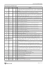
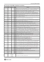
 Pin Functions of the DIO mode

Pin name

Pin number

Logic

I/O

Function

DEC1UF

3

--

--

Connect a capacitor whose ef

fective capacitance is at least 1 μF and a 0.1 μF ceramic capacitor 

for high frequency bypass in parallel between this pin and V

SS

.  Or connect a laminated ceramic 

capacitor of around 2.2 μF with the property that capacitance reduction is about 20% even in 

DC bias.

#Reset

6

Negative I/O The hardware reset input pin of MKY44-IO32A.  Right after power is turned on or when the 

user intentionally resets the hardware, Low should be retained for at least 200 μs.

IOSWAP

7

Positive

I

Input pin for the setting that inverts the “input” or “output” status of the 32 general-purpose I/

O pins determined by the settings of IOS0 and IOS1.  If the Low-level is set when this pin is 

High-level, “input” will be inverted to “output,” and vice versa.  The setting status of this pin is 

read when returning from a hardware reset.

XTAL4i

XTAL4o

10,11

--

--

Pins to connect a crystal oscillator.  Connect a 4 MHz crystal oscillator between these pins.  

Connect 20 pF ceramic capacitors between these pins and V

SS

.  Connect them near the pins.

DIP_ON

15

Positive

O

Connect this pin with pin DIP_ON of the ST44SW.  For more information about the ST44SW, 

refer to the ST44SW User’s Manual.

DIP_RX

17

Positive

I

Connect this pin with pin DIP_TX of the ST44SW.  For more information about the ST44SW, 

refer to the ST44SW User’s Manual.

Io30 to Io37

16

18 to 22

24, 25

Positive

I/O

Pins corresponding to bits 24 to 31 among the 32 bits of general-purpose I/O pins.

Leave this pin open when not in use.

Io00 to Io07

27 to 34

Positive

I/O

Pins corresponding to bits 0 to 7 among the 32 bits of general-purpose I/O pins.

Leave this pin open when not in use.

Io10 to Io17

35 to 42

Positive

I/O

Pins corresponding to bits 8 to 15 among the 32 bits of general-purpose I/O pins.

Leave this pin open when not in use.

Io20 to Io27

43 to 46

59 to 62

Positive

I/O

Pins corresponding to bits 16 to 23 among the 32 bits of general-purpose I/O pins.

Leave this pin open when not in use.

ChipMode

26

Positive

I

Pin to set the mode of the MKY44-IO32A.  To use it as described in this data sheet, be sure to 

retain the High-level by connecting to Vdd.

DONA

47

Positive

O

This pin retains the High-level during the DONA (DO Not Arrival) state.

It is at Low-level at other times.

STB2

48

Positive

O

Outputs a High-level pulse when reading in the status of the general-purpose input pins.

The MKY44-IO32A reads in the status of the general-purpose input pins while this pin is High.

STB1

50

Positive

O

Outputs a High-level pulse when updating the status of the general-purpose output pins.

The MKY44-IO32A updates the status of the general-purpose output pins while this pin in High.

IOS0

51

Positive

I

Pins to set the “input” or “output” status of the 32 general-purpose I/O pins.  Using a 

combination of High-level and Low-level input to this pin, “input” or “output” is set for the 32 

general-purpose I/O pins.  The setting status of these two pins (IOS0 and IOS1) is read when 

returning from a hardware reset.

IOS1

52

#MCARE

53

Negative

O

A pin to output the MCARE signal, which is a standard function of CUnet.  This pin outputs the 

Low-level for about 50 ms, when the MCARE signal occurs and when it returns from hardware 

reset.

#LCARE

54

Negative

O

A pin to output the LCARE signal, which is a standard function of CUnet.  This pin outputs the 

Low-level for about 50 ms, when the LCARE signal occurs and when it returns from hardware 

reset.

It is recommended to connect orange color LED indicating a gentle warning to this pin.

#MON

55

Negative

O

A pin to output the MON signal, which is a standard function of CUnet.  This pin retains Low-

level while a link has been established with another CUnet devices for at least 3 consecutive 

cycles.

It is recommended to connect green color LED indicating a stable operation to this pin.

CU_TXD

56

Positive

O

Output pin to send CUnet packets.

Connect this pin to a drive input pin such as of a driver.

CU_TXE

57

Positive

O

A pin to output the High-level while CUnet packets are output.  

Connect this pin to the enable input pin of the driver.

CU_RXD

58

Positive

I

A pin to input CUnet packets.

Connect this pin to the output pin of the receiver.

Vdd

1, 2, 4, 23

--

--

Power pin.  Supply 3.3 V.

Vss

5, 9, 12

--

--

Power pin.  Connected to 0 V.

N.C.

8, 13, 14, 

49, 63, 64

--

--

Do not connect to other signals; keep them open.

Содержание CUnet MKY44-IO32A

Страница 1: ...rature range 40 to 85 C Package 64 pin TQFP 0 5 mm pitch 10 mm 10 mm ST44SW Required Applications Industrial devices Medical devices Measurement devices Power wire monitoring Process control Overview...

Страница 2: ...to DIO Mode PWM and Up Down Counter Mode RX FDQ VHW WKH LQSXW RI WKH 0 2 WR JR WKURXJK XS WR GLJLWDO OWHUV E WXUQLQJ 21 WKH RQ ELW RI 3 6 7KH IDFWRU GHIDXOW VDPSOH LQWHUYDO RI WKH 0 2 LV V 7KXV VLJQD...

Страница 3: ...Do4 Do4 R L L L L R R R R R R L L L L R R R R R R L L L L R R R R R R Do8 Di8 Di8 Di8 R Di8 Do8 Do8 Do8 R Do9 Di9 Di9 Di9 R Di9 Do9 Do9 Do9 R R L L L R L R R R R R L L L R L R R R R R L L L R L R R R...

Страница 4: ...V 21 32 3 DOHL 2 VHWWLQJ WR VHOHFW WKH RXWSXW GDWD WR WKH RXWSXW SLQ 7KH ORZHU ELWV LQ WKH PHPRU EORFN DUH VHOHFWHG ZKHQ WKH 3 6 LV LQ WKH 2 VWDWH 7KH XSSHU ELWV LQ WKH PHPRU EORFN DUH VHOHFWHG ZKHQ 3...

Страница 5: ...1 60 59 58 57 56 55 54 53 52 51 50 49 48 Content 0 FI9 FI13 FI12 FI11 FI10 FI8 FI7 FI6 FI5 FI4 FI3 FI2 FI1 FI0 Setting values are stored in bits 32 to 63 These bits show the following settings loaded...

Страница 6: ...RI WKH 0 2 VHWV WKH 2 VHOHFWLRQV IRU WKH JHQHUDO SXUSRVH 2 SLQV XVLQJ SLQV 26 26 DQG 26 3 7KH XVH RI WKH 0 2 UHTXLUHV WKH 67 6 D GHGLFDWHG 6 WR ORDG WKH 3 6 VHWWLQJV 7KH 0 2 RSHUDWHV E UHDGLQJ YLD WK...

Страница 7: ...n to set the mode of the MKY44 IO32A To use it as described in this data sheet be sure to retain the High level by connecting to Vdd DONA 47 Positive O This pin retains the High level during the DONA...

Страница 8: ...it 6WRUDJH WHPSHUDWXUH 7VWJ 2SHUDWLQJ WHPSHUDWXUH 7RSU 3LQ YROWDJH DEVROXWH PD LPXP UDWLQJ VI 9DD 9 2SHUDWLQJ SRZHU VXSSO YROWDJH 9DD 9 0HDQ RSHUDWLQJ FXUUHQW 9DDA 9L 9DD RU 9SS RXWSXW RSHQ 7 0 mA 2 S...

Страница 9: ...B 7 I IOSWAP A 23 Vdd 39 I O Io14 A B 55 O MON B 8 N C 24 I O Io36 A B 40 I O Io15 A B 56 O CU_TXD B 9 VSS 25 I O Io37 A B 41 I O Io16 A B 57 O CU_TXE B 10 XTAL4i 26 I ChipMode A 42 I O Io17 A B 58 I...

Страница 10: ...Page 10 22 CUnet Family MKY44 IO32A XQFWLRQ ORFNV RI 3 0 DQG 8S RZQ RXQWHU 0RGH 7KH IROORZLQJ VKRZV WKH IXQFWLRQ EORFNV LQ WKH 3 0 DQG 8S RZQ FRXQWHU PRGH RI WKH 0 2...

Страница 11: ...JLWDO OWHU IRU WKH LQSXW VLJQDO KHQ WKH 3 6 LV LQ WKH 21 VWDWH WKH GLJLWDO OWHU LV 21 32 3 G F RQ W DUH 7KH VHWWLQJ RI WKLV VZLWFK GRHV QRW PDWWHU LQ 3 0 DQG 8S RZQ FRXQWHU PRGH 3 DOSA 26 6HW 26 YDOXH...

Страница 12: ...Content Di7 Di6 Di5 Di4 Di3 Di2 Di1 Di0 CUT0 23 CUT0 22 CUT0 21 CUT0 20 CUT0 19 CUT0 18 CUT0 17 CUT0 16 Bit 47 46 45 44 43 42 41 40 39 38 37 36 35 34 33 32 Content CUT1 15 CUT1 14 CUT1 13 CUT1 12 CUT...

Страница 13: ...9 3 0 8 3 0 3 0 3 0 3 0 4 3 0 3 3 0 2 3 0 3 0 LW 49 48 Content R R R Do4 Do3 Do2 R R G F 7KH YDOXH LQ GRQ W FDUH G F ZLOO QRW DIIHFW WKH RSHUDWLRQ RI WKH 0 2 Q WKH H DPSOH RI JHQHUDWLRQ RI 3 0 RXWSXW...

Страница 14: ...WKH FRQQHFWLRQV LQ WKH 3 0 DQG 8S RZQ FRXQWHU PRGH RI WKH 0 2 7KH XVH RI WKH 0 2 UHTXLUHV WKH 67 6 D GHGLFDWHG 6 WR ORDG WKH 3 6 VHWWLQJV 7KH 0 2 RSHUDWHV E UHDGLQJ YLD WKH 67 6 WKH VHWWLQJV RI VWDWLR...

Страница 15: ...vel 1 is added to the value of counter 1 Leave this pin open when not in use DOWN1 39 Negative I Count down input pin of counter 1 When the signal of this pin transits from High level to Low level 1 w...

Страница 16: ...7 S Max Unit 6WRUDJH WHPSHUDWXUH 7VWJ 2SHUDWLQJ WHPSHUDWXUH 7RSU 3LQ YROWDJH DEVROXWH PD LPXP UDWLQJ VI 9DD 9 2SHUDWLQJ SRZHU VXSSO YROWDJH 9DD 9 0HDQ RSHUDWLQJ FXUUHQW 9DDA 9L 9DD RU 9SS RXWSXW RSHQ...

Страница 17: ...MCARE B 6 I Reset C 22 O Do5 B 38 I UP1 A 54 O LCARE B 7 N C 23 VDD 39 I DOWN1 A 55 O MON B 8 N C 24 O Do6 B 40 I CLR1 A 56 O CU_TXD B 9 VSS 25 O Do7 B 41 O PWM0 B 57 O CU_TXE B 10 XTAL4i 26 I ChipMo...

Страница 18: ...UHFRPPHQGHG WR FRQQHFW RUDQJH FRORU SDUW LQGLFDWLQJ D JHQWOH ZDUQLQJ 7R 0 5 SLQ LW LV UHFRPPHQGHG WR FRQQHFW UHG FRORU SDUW LQGLFDWLQJ D GH QLWH ZDUQLQJ 7KHVH SLQV KDYH r P FXUUHQW GULYH FDSDELOLW RQ...

Страница 19: ...n Valid range 91 9Q 9HUVLRQ 1XPEHU 6KRZV WKH YHUVLRQ QXPEHU RI WKH 0 2 LQ WZR 6 FKDUDFWHUV 7KH YHUVLRQ QXPEHUV VWDUW IURP 91 UHSUHVHQWV WKH WHQV SODFH DQG 9Q UHSUHVHQWV WKH RQHV SODFH WR in ASCII SA 3...

Страница 20: ...ZDUH UHVHW LV H HFXWHG WKH 0 2 ZLOO VWDUW RSHUDWLRQ DFFRUGLQJ WR WKH YDOXHV VWRUHG LQ WKH DVK 520 I WKH 0 2 FRXOG QRW FKDQJH WKH VHWWLQJ VXFFHVVIXOO XVLQJ WKH PDLO IXQFWLRQ LW ZLOO UHWXUQ D 1 FRGH PHV...

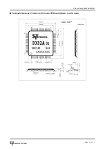
Страница 21: ...Page 21 22 CUnet Family MKY44 IO32A 3DFNDJH LPHQVLRQV RPPRQ WR 2 PRGH 3 0 DQG 8S RZQ FRXQWHU PRGH...

Страница 22: ...nts and any other rights of a third party 4 When using this product and the information and circuits in this data sheet we do not guarantee the right to use any property rights intellectual property r...

Отзывы: