XAV-60/E60
57
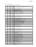
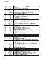
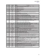
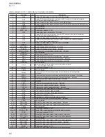
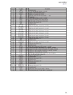
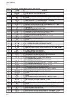
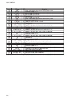
Pin No.
Pin Name
I/O
Description
1 to 9
MEMDAT2 to
MEMDAT7,
MEMDAT13 to
MEMDAT15
I/O
Two-way data bus with the fl ash memory
10
VDDC
-
Power supply terminal (+1.8V)
11
VDDP
-
Power supply terminal (+3.3V)
12
MEMADD16
O
Address signal output to the fl ash memory
13
MEMCS1
O
Chip select signal output to the fl ash memory
14 to 21
MEMADD15 to
MEMADD8
O
Address signal output to the fl ash memory
22
MEMWR#
O
Write enable signal output to the fl ash memory
23 to 29
MEMADD18,
MEMADD17,
MEMADD7 to
MEMADD3
O
Address signal output to the fl ash memory
30
VDDP
-
Power supply terminal (+3.3V)
31 to 33
MEMADD2,
MEMADD1,
MEMADD19
O
Address signal output to the fl ash memory
34
USBVBUS
-
USB VBUS terminal Not used
35
USBID
I/O
USB identifi cation signal input/output terminal Not used
36
USBVDDA3P3
-
Power supply terminal (+3.3V)
37
USBDP
I/O
Two-way USB data (positive) with the USB connector
38
USBDN
I/O
Two-way USB data (negative) with the USB connector
39
USBREF
O
USB reference voltage output terminal Not used
40
USBXO
O
System clock output terminal (12 MHz) (for USB)
41
USBXI
I
System clock input terminal (12 MHz) (for USB)
42
USBVSSPLL
-
Ground terminal
43
USBVDDPLL1V8
-
Power supply terminal (+1.8V)
44 to 46
RAMADD3 to
RAMADD5
O
Address signal output to the SD-RAM
47
VDDIP
-
Power supply terminal (+3.3V)
48 to 51
RAMADD2,
RAMADD6,
RAMADD1,
RAMADD7
O
Address signal output to the SD-RAM
52
VDDC
I
Power supply terminal (+1.8V)
53 to 55
RAMADD0,
RAMADD8,
RAMADD10
O
Address signal output to the SD-RAM
56
VDDP
-
Power supply terminal (+3.3V)
57
GNDC
-
Ground terminal
58, 59
RAMADD9,
RAMADD11
O
Address signal output to the SD-RAM
60
RAMCS0#
O
Chip select signal output to the SD-RAM
61
RAMBA
O
Bank address signal output to the SD-RAM
62
RAMCS1#
O
Chip select signal output to the SD-RAM
63
RAMRAS#
O
Row address signal output to the SD-RAM
64
RAMCAS#
O
Column address signal output to the SD-RAM
65
VDDP
-
Power supply terminal (+3.3V)
66
GNDC
-
Ground terminal
67
RAMWE#
O
Write enable signal output to the SD-RAM
68
RAMDQM
O
Data mask signal output to the SD-RAM
69
GNDPCLK
-
Ground terminal
70
PCLK
O
Clock signal output to the SD-RAM
71
VDDPCLK
-
Power supply terminal (+3.3V)
72 to 75
RAMDAT9 to
RAMDAT6
I/O
Two-way data bus with the SD-RAM
76
VDDP
-
Power supply terminal (+3.3V)
77
GNDC
-
Ground terminal
• IC Pin Function Description
SERVO BOARD IC4 ZR36988HQCG-A (DVD PROCESSOR)
Содержание XAV-60 - 6.1 Inch Avc
Страница 92: ...92 XAV 60 E60 MEMO ...

