


2
STR-KS1100
SAFETY-RELATED COMPONENT WARNING!!
COMPONENTS IDENTIFIED BY MARK
0
OR DOTTED LINE
WITH MARK
0
ON THE SCHEMATIC DIAGRAMS AND IN
THE PARTS LIST ARE CRITICAL TO SAFE OPERATION.
REPLACE THESE COMPONENTS WITH SONY PARTS WHOSE
PART NUMBERS APPEAR AS SHOWN IN THIS MANUAL OR
IN SUPPLEMENTS PUBLISHED BY SONY.
TABLE OF CONTENTS
1.
GENERAL
...................................................................
3
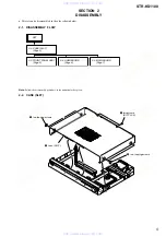
2.
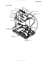
DISASSEMBLY
2-1.
Disassembly Flow ...........................................................
5
2-2.
Case (SL07) .....................................................................
5
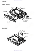
2-3.
Front Panel Assy ..............................................................
6
2-4.
HDMI Board ....................................................................
6
2-5.
MAIN Board ....................................................................
7
3.
TEST MODE
..............................................................
8
4.
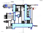
DIAGRAMS
4-1.
Block Diagram – MAIN Section – .................................
9
4-2.
Block Diagram – AMP Section – ................................... 10
4-3.
Block Diagram – HDMI Section – ................................. 11
4-4.
Block Diagram
– PANEL/POWER SUPPLY Section – ........................... 12
4-5.
Schematic Diagram – I/O Board – ................................. 15
4-6.
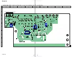
Printed Wiring Board
– I/O Board (Component Side) – ................................... 16
4-7.
Printed Wiring Board
– I/O Board (Conductor Side) – ...................................... 17
4-8.
Printed Wiring Board
– MAIN Board (Component Side) – ............................... 18
4-9.
Printed Wiring Board
– MAIN Board (Conductor Side) – ................................. 19
4-10. Schematic Diagram – MAIN Board (1/8) – ................... 20
4-11. Schematic Diagram – MAIN Board (2/8) – ................... 21
4-12. Schematic Diagram – MAIN Board (3/8) – ................... 22
4-13. Schematic Diagram – MAIN Board (4/8) – ................... 23
4-14. Schematic Diagram – MAIN Board (5/8) – ................... 24
4-15. Schematic Diagram – MAIN Board (6/8) – ................... 25
4-16. Schematic Diagram – MAIN Board (7/8) – ................... 26
4-17. Schematic Diagram – MAIN Board (8/8) – ................... 27
4-18. Printed Wiring Boards – DCAC/SPEAKER Boards – ... 28
4-19. Schematic Diagram – DCAC/SPEAKER Boards – ....... 29
4-20. Printed Wiring Board – HDMI Board – ......................... 30
4-21. Schematic Diagram – HDMI Board – ............................ 31
4-22. Printed Wiring Boards – PANEL Section – .................... 32
4-23. Schematic Diagram – PANEL Section – ........................ 33
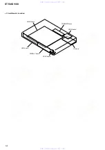
5.
EXPLODED VIEWS
5-1.
Overall Section ................................................................ 49
5-2.
MAIN Section ................................................................. 50
6.
ELECTRICAL PARTS LIST
................................ 51
General
Power requirements
Power output (DIGITAL MEDIA PORT)
DC OUT:
5 V, 700 mA
Power consumption
Power consumption (during standby mode)
0.3 W
Dimensions (w/h/d) (Approx.)
430
×
66.5
×
335 mm
including projecting parts
and controls
Mass (Approx.)
3.6 kg
Area code
Power requirements
CEL, CEK
230 V AC, 50/60 Hz
Area code
Power consumption
CEL, CEK
110 W
Design and specifications are subject to
change without notice.
UNLEADED SOLDER
Boards requiring use of unleaded solder are printed with the lead-
free mark (LF) indicating the solder contains no lead.
(Caution: Some printed circuit boards may not come printed with
the lead free mark due to their particular size)
: LEAD FREE MARK
Unleaded solder has the following characteristics.
•
Unleaded solder melts at a temperature about 40 ˚C higher
than ordinary solder.
Ordinary soldering irons can be used but the iron tip has to be
applied to the solder joint for a slightly longer time.
Soldering irons using a temperature regulator should be set to
about 350 ˚C.
Caution: The printed pattern (copper foil) may peel away if
the heated tip is applied for too long, so be careful!
Strong viscosity
Unleaded solder is more viscou-s (sticky, less prone to flow)
than ordinary solder so use caution not to let solder bridges
occur such as on IC pins, etc.
Usable with ordinary solder
It is best to use only unleaded solder but unleaded solder may
also be added to ordinary solder.
Notes on chip component replacement
•
Never reuse a disconnected chip component.
•
Notice that the minus side of a tantalum capacitor may be
damaged by heat.
www. xiaoyu163. com
QQ 376315150
9
9
2
8
9
4
2
9
8
TEL 13942296513
9
9
2
8
9
4
2
9
8
0
5
1
5
1
3
6
7
3
Q
Q
TEL 13942296513 QQ 376315150 892498299
TEL 13942296513 QQ 376315150 892498299


