


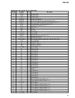


42
PRS-500
Pin No.
Pin Name
I/O
Description
J12
VSS
—
Ground
J13
TST3
I
AutOmode (normal = “0”)(Not used (Fixed to “L”))
J14
H_D5
I/O
8 bits data bus for main CPU
J15
H_D4
I/O
8 bits data bus for main CPU
K1
A16
O
22 bits address bus
K2
A15
O
22 bits address bus
K3
F_NRST
O
N reset for Flash
K4
VSS
—
Ground
K12
VSS
—
Ground
K13
TST2
I
Test mode (normal = “0”)(Not used (Fixed to “L”))
K14
H_D3
I/O
8 bits data bus for main CPU
K15
H_D2
I/O
8 bits data bus for main CPU
L1
A20
O
Not used (Open)
L2
A17
O
22 bits address bus
L3
A21
O
Not used (Open)
L4
VDD
—
+3V0
L12
VSS
—
Ground
L13
NPOR
I
Power on reset
L14
H_D1
I/O
8 bits data bus for main CPU
L15
H_D0
I/O
8 bits data bus for main CPU
M1
VDD
—
+3V0
M2
A19
O
Not used (Open)
M3
F_RDY
I
Ready for Flash
M4
VDD
—
+3V0
M5
VSS
—
Ground
M6
VSS
—
Ground
M7
VDD
—
+3V0
M8
n.c.
—
Not used (Open)
M9
VSS
—
Ground
M10
VSS
—
Ground
M11
n.c.
—
Not used
M12
VDD
—
+3V0
M13
BORDER0
O
Border control
M14
H_ACK
O
Acknowledge for main CPU
M15
H_DS
I
Device select from main CPU
N1
D0
I/O
32 bits data bus
N2
VSS
—
Ground
N3
D2
I/O
32 bits data bus
N4
VDD
—
+3V0
N5
BIST_EN
I
Bist enable (Not used (Fixed to “L”))
N6
F_NWE
O
Write enable for Flash
N7
n.c.
—
Not used (Open)
N8
VSS
—
Ground
N9
VDD
—
+3V0
N10
VSS
—
Ground
N11
CLK
I
Clock input
N12
CLK_OUT
O
Clock output
N13
COM_CTRL
O
Common control
N14
PWR_NEG
O
Negative power