


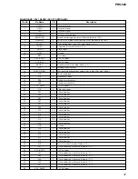


33
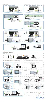
PRS-500
• IC Pin Function Description
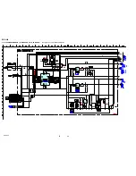
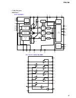
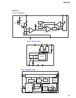
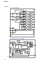
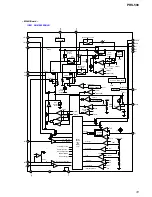
MAIN BOARD IC1001 MC9328MXLVP20R2 (MAIN CPU)
Pin No.
Pin Name
I/O
Description
A1
SD_CMD
O
Not used (Open)
A2
SRAMINT
I
Not used (Fixed to “H”)
A3
VBUS
I
VBUS input
A4
USBD_OE
O
USB output enable
A5
USBD_SUSPND
O
USB suspend
A6
USBD_VM
I
USB minus input
A7
SSI_RXFS
I
Not used (Open)
A8
SSI_TXCLK
O
Serial clock output for audio DAC
A9
NAND
-
CE1
O
Not used
A10
NAND
-
CE0
O
Chip enable for NAND Flash ROM
A11
SDINT
I
SD interrupt input
A12
PD9
—
Not used (Open)
A13
PCEINK
—
Not used (Open)
A14
DS1
O
Device select output for indicator controller
A15
DS2
O
Not used (Open)
B1
SD_DAT3
I/O
Not used (Open)
B2
SD_CLK
O
Not used (Open)
B3
SD_DET
I
SD card detect input
B4
USBD_AFE
O
Not used (Open)
B5
USBD_RCV
I
USB receive data input
B6
USBD_VMO
O
USB minus output
B7
SSI_RXDAT
I
Not used (Fixed to “L”)
B8
UART1_TXD
O
Serial data output for sub CPU
B9
RY//BY
I
Ready/Busy input from NAND Flash ROM
B10
LSCLK
O
Not used (Open)
B11
HPSET
I
Head phone detect input
B12
PCETHER
—
Not used (Open)
B13
PCDSP
—
Not used (Open)
B14
ACK
I
Acknowledge from indicator controller
B15
C/D
O
Command/data output for indicator controller
C1
D31
I/O
32 bits data bus
C2
SD_DAT0
I/O
Not used (Open)
C3
MSINT
I
MS interrupt input
C4
SD_WP
I
SD write protect input
C5
SD_DAT2
I/O
Not used (Open)
C6
USBD_VPO
O
USB plus output
C7
UART2_RXD
I
Not used (Fixed to “H”)
C8
SSI_TXFS
O
LRCK output for audio DAC
C9
UART1_RTS
I
Serial request from sub CPU
C10
USB_BOOT
I
USB boot mode input
C11
PCMS
O
Power controll output for SD/MS
C12
R/W
O
Read/write enable output for indicator controller
C13
WUP
O
Wake up output for indicator controller
C14
SRETHER
O
Not used
C15
NVDD2
—
2.9V DC input
D1
A23
O
25 bits address bus
D2
A24
O
25 bits address bus