– 43 –
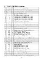
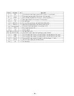
Pin No.
Pin Name
I/O
Description
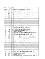
103
XLRF
O
Serial latch signal output terminal Not used (open)
104
CKRF
O
Serial clock signal output terminal Not used (open)
105
DTRF
O
Write data output terminal Not used (open)
106
APCREF
O
Control signal output to the reference voltage generator circuit for the laser automatic power
control
107
LDDR
O
PWM signal output for the laser automatic power control Not used (open)
108
VDC4
—
Power supply terminal (+1.7V) (for internal logic)
109
TRDR
O
Tracking servo drive PWM signal (–) output to the XC111256FTA (IC551)
110
TFDR
O
Tracking servo drive PWM signal (+) output to the XC111256FTA (IC551)
111
FFDR
O
Focus servo drive PWM signal (+) output to the XC111256FTA (IC551)
112
FRDR
O
Focus servo drive PWM signal (–) output to the XC111256FTA (IC551)
113
FS4
O
Clock signal output terminal (X' tal system 176.4 kHz) Not used (open)
114
SRDR
O
Sled servo drive PWM signal (–) output terminal Not used (open)
115
SFDR
O
Sled servo drive PWM signal (+) output terminal Not used (open)
116
VSC4
—
Ground terminal (for internal logic)
117
SPRD
O
Spindle servo drive PWM signal (–) output terminal Not used (open)
118
SPFD
O
Spindle servo drive PWM signal (+) output terminal Not used (open)
119
FGIN
I
FG signal input terminal for spindle servo Not used (open)
120 to 122 TEST1 to TEST3
I
Input terminal for the test (normally : fixed at “L”)
123
MTFLGR
O
Muting applied to analog signal input in non-signal status causes the signal to be “H”
automatically Not used (open)
124
SPVS
O
Spindle servo drive voltage control signal output to the XC111256FTA (IC551)
125
VDI03
—
Power supply terminal (+2.4V) (for I/O cell)
126
VSI03
—
Ground terminal (for I/O cell)
127
SPDU
O
Spindle servo (U) drive signal output to the XC111256FTA (IC551)
128
SPDV
O
Spindle servo (V) drive signal output to the XC111256FTA (IC551)
129
SPDW
O
Spindle servo (W) drive signal output to the XC111256FTA (IC551)
130
SPCU
I
Spindle servo (U) timing signal input from the XC111256FTA (IC551)
131
SPCV
I
Spindle servo (V) timing signal input from the XC111256FTA (IC551)
132
SPCW
I
Spindle servo (W) timing signal input from the XC111256FTA (IC551)
133
SLDU
O
Sled servo (1+) drive signal output to the XC111256FTA (IC551)
134
SLDV
O
Sled servo (1–) drive signal output to the XC111256FTA (IC551)
135
SLDW
O
Sled servo (2+) drive signal output to the XC111256FTA (IC551)
136
VDC5
—
Power supply terminal (+1.7V) (for internal logic)
137
VSC5
—
Ground terminal (for internal logic)
138
SLCU
I
Sled servo (1) timing signal input from the XC111256FTA (IC551)
139
SLCV
I
Sled servo (2) timing signal input from the XC111256FTA (IC551)
140
SLCW
O
Sled servo (2–) timing signal output to the XC111256FTA (IC551)
141
SLVS
O
Sled servo voltage control signal output to the XC111256FTA (IC551)
142
BYPS
O
By-pass transistor control signal output terminal Not used (open)
143
DVSSDRAM
—
Ground terminal (for internal 16M bit D-RAM)
144
DVDDDRAM
—
Power supply terminal (+2.4V) (for internal 16M bit D-RAM)
145
DVSSDRAM
—
Ground terminal (for internal 16M bit D-RAM)
146
DVDDDRAM
—
Power supply terminal (+2.4V) (for internal 16M bit D-RAM)
147 to 168
NC
—
Not used (open)

