39
6-6-4. Auto Check
(See page 42)
Start
YES
NO
NO
NO
NO
NO
NO
NO
NO
YES
YES
YES
YES
YES
YES
YES
Replace IC195
Replace OP or IC195
Replace IC101, IC195, or D101
6-11. Iop NV SAVE (See page 45)
Replace OP, IC190, or IC195
Replace OP, IC102, IC190,
or IC195
Replace OP, IC101, IC151,
or IC195
Replace OP
Replace the spindle motor
End adjustments
After turning off and then on the power,
initialize the EEPROM
For details, refer to 4-11. WHEN MEMORY NG IS
DISPLAYED (See page 32)
• Abbreviation
OP: Optical pick-up
6-7. INITIAL SETTING OF ADJUSTMENT VALUE
(See page 44)
6-9. TEMPERATURE COMPENSATION OFFSET
ADJUSTMENT (See page 44)
6-10. LASER POWER ADJUSTMENT (See page 44)
6-12. TRAVERSE ADJUSTMENT (See page 45)
6-13. FOCUS BIAS ADJUSTMENT (See page 46)
6-16. AUTO GAIN CONTROL OUTPUT LEVEL
ADJUSTMENT (See page 47)
OP change in Err Display mode
Iop write
Spindle change in Err Display mode
Adjustment flow
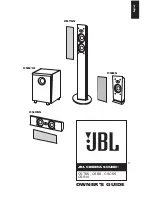
Содержание HCD-VZ50MD
Страница 8: ...8 BD CD board BD CD BOARD To repair the BD CD board remove the bottom plate Bottom view ...
Страница 57: ...HCD VZ50MD 57 57 7 4 SCHEMATIC DIAGRAM DECK SECTION E Page 64 TO MAIN BOARD 16 ...
Страница 59: ...HCD VZ50MD 59 59 7 6 SCHEMATIC DIAGRAM CD SECTION See page 50 for Waveforms See page 90 for IC Block Diagrams ...
Страница 64: ...HCD VZ50MD 64 64 7 11 SCHEMATIC DIAGRAM MAIN 1 4 SECTION ...
Страница 65: ...HCD VZ50MD 65 65 7 12 SCHEMATIC DIAGRAM MAIN 2 4 SECTION See page 89 for IC Block Diagrams ...
Страница 67: ...HCD VZ50MD 67 67 7 14 SCHEMATIC DIAGRAM MAIN 4 4 SECTION See page 89 for IC Block Diagrams ...
Страница 71: ...HCD VZ50MD 71 71 7 18 SCHEMATIC DIAGRAM DIGITAL 2 2 SECTION See page 92 for IC Block Diagrams ...
Страница 73: ...HCD VZ50MD 73 73 7 20 SCHEMATIC DIAGRAM AMP SECTION ...
Страница 77: ...HCD VZ50MD 77 77 7 24 SCHEMATIC DIAGRAM SWITCH SECTION ...
Страница 83: ...HCD VZ50MD 83 83 7 32 SCHEMATIC DIAGRAM POWER SUPPLY SECTION ...