


Developer's Board Manual Rev A
Page 26 of 28
SEM/CX-02:0061/MAN
4 Troubleshooting
Your
Application
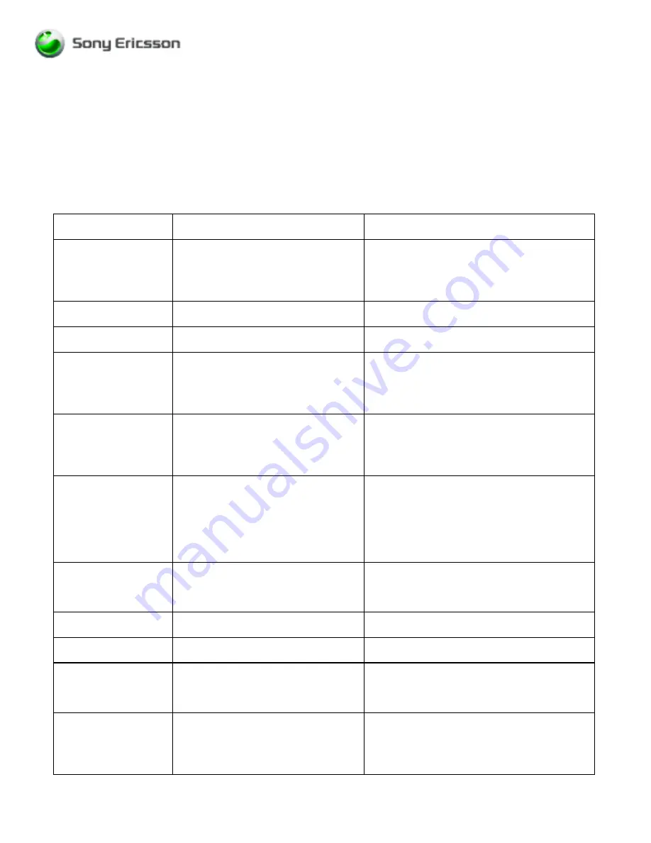
4.1 System Connector Header
The application can use the 40-pin header connector to interface to the module.
The pin numbering of the header connector is the same as for the 40-pin system connector.
Both the application and the development system can drive most of the input pins to the module. The exception
is CTMS, see below.
Pin Number / Name
Description
Application usage & priority together with a
development system
2 / VREF
Module logic voltage reference output
from the module. The application shall
use this voltage, current amplified, as
supply for its logic interface circuitry
towards the module.
The application and the development system
can use this signal at the same time.
7 / AFMS
Audio output from module to the
application.
The application and the development system
can use this signal at the same time.
9 / AGND
Analog reference for both ATMS and
AFMS.
The application and the development system
can use this signal at the same time.
10 / ATMS
Audio input to module from the
application.
Set switch S201 to “BYPASS” when driving this
signal from the application. Disconnect ATMS
from the application and set switch S201 to
“PRE-AMP” when using the development
board headset.
12 /
MODULE_PWR_EN_B
Open collector input to the module that
held active low, enables the main
supply voltage for the module.
The device holding this signal active low will
control the operation.
Switch S3:6 “WAKE” must be set to OFF
position if the application wants to control the
power of the module.
15 / HW_SD
Open collector output and CMOS input
in both directions (module –
application). This signal is pulled up
inside the module.
A low level for more than 100ms will
trigger the module to perform a
shutdown.
The application and the development system
can use this signal at the same time.
23 / VPPFLASH_DCD
Flash request input to module at
startup. DCD output from module after
initialization.
The application and the development system
can use this signal at the same time.
The module will enter Flash-mode if the signal
is held high at startup.
24 / RINGER
PWM output from module that
generates ring signals.
The application and the development system
can use this signal at the same time.
25 / CTS
Clear To Send
The application and the development system
can use this signal at the same time.
26 / DTR
Data Terminal Ready
The application will take control of this signal
when connected. The application must be
capable of handling a 1k ohm load unless
switch S3:3 is set to “OFF”.
27 / DTMS
Data To Module Station.
The application and the development system
can use this signal at the same time, but data
will be corrupted if it is sent from both the
application and the J2 interface at the
simultaneously.