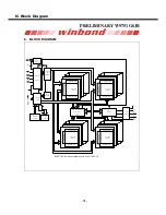
IC Block Diagram
-
28
-
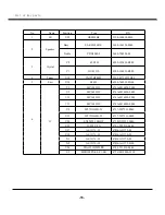
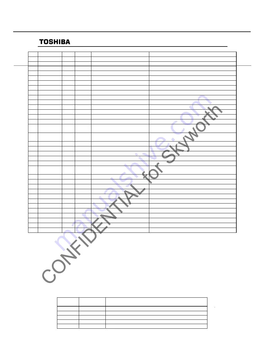
TC90517FG Toshiba products specification [Tentative]
CONFIDENTIAL
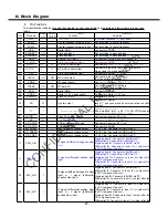
DC component was cut.
31
AD_DVSS
-
-
ADC digital
GND
Connects to DGND
.
32
AD_ DVDD
-
-
ADC digital power supply
Connects to d2.5 V typ.
33
VSS
-
-
Digital GND
Connects to DGND
.
34
DR1VDD
-
-
D1.2 V power supply
Connects to d1.2 V typ.
35
VDDS
-
-
I/O power supply
Con nects to d3
.
3 V typ
.
36
VDDC
-
-
D1.2 V power supply
Connects to d1.2 V typ.
37
VSS
-
-
Digital GND
Connects to DGND
.
38
STSFLG1
O
PD
Status flag 1 output
Open, fixed to L when not used.
39
DTCLK
I
PD
Pin for pre-shipment test
Open or connects to DGND.
40
DTMB
I
PU
Pin for pre-shipment test
Open or connects to d3.3 V typ.
41
TSMD1
I
-
Pin for pre-shipment test
Connects to DGND.
42
SYRSTN
I/O
OD
System reset input
Input
at specified timing at power ON.
43
DR2VDD
-
-
D2.5 V power supply
Connects to d2.5 V typ.
44
VSS
-
-
Digital GND
Connects to DGND
.
45
SCL
I/O
OD
I2C clock input for host CPU
Connects to I2C clock bus.
(Pull-up performed outside IC
.
)
46
SDA
I/O
OD
I2C data I/O for host CPU
Connects to I2C data bus.
(Pull-up performed outside IC
.
)
47
VSS
-
-
Digital GND
Connects to DGND.
48
DR1VDD
-
-
D1.2 V power supply
Connects to d1.2 V typ.
49
VDDS
-
-
I/O power supply
Con nects to d3
.
3 V typ
.
50
VSS
-
-
Digital GND
Connects to DGND
.
51
STSFLG0
I/O
PD
Status flag 0 output
Open, fixed to L when not used.
52
SLOCK
O
Synchronization completion
(sequence 8 or higher) flag
Open, fixed to L when not used.
53
RERR
O
-
RS decoding error flag output
Open, fixed to L when not used.
54
RLOCK
O
-
RS decoding error free flag output
Open, fixed to L when not used.
55
RSEORF
O
-
TS error flag output
Open, fixed to L when not used.
56
VDDC
-
-
D1.2 V power supply
Connects to d1.2 V typ.
57
VSS
-
-
Digital GND
Connects to DGND.
58
PBVAL
O
-
TS valid flag output
Open, fixed to L when not used.
59
SBYTE
O
-
TS synchronization byte flag output Open, fixed to L when not used.
60
SRDT
O
-
Serial TS data output
-
61
SRCK
O
-
TS serial clock output
-
62
VSS
-
-
Digital GND
Connects to DGND
.
63
VDDC
-
-
D1.2 V power supply
Connects to d1.2 V typ.
64
VDDS
-
-
I/O power supply
Con
nects to d3.3 V typ.
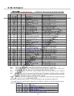
Note 2
AGND is the abbreviation for analog GND, and DGND is the abbreviation for digital GND.
Note 3
The test dedicated pin is used for the pre-shipment test only. Make sure that processing is performed as
indicated in the "Remarks" column. Any other method will lead to malfunction or failure.
Note 4
I/O indicates the type of the cell used. It may be different from the pin function because a test is conducted
concurrently
.
Note 5
PU indicates an I/O with a pull-up resistor (50 k
typ.) and PD indicates an I/O with a pull-down resistor (50
k
typ.). Pulling down the PU pin or pulling up the PD pin outside the IC sometimes changes the electric
potential to the midpoint, resulting in instability. Caution is required.
Note 6
The unused output pins must be open and fixed to L by setting the output enable control register of each pin
for noise reduction or set
to the output OFF state.
Note 7
OD indicates an open drain I/O. To use the pin for output, pull up the resistance outside the IC.
* The following pins are added with the upgrade from TC90507 to TC90517 (except the changes of power
supply and GND pins):
Pin
Number
Pin Name
Description
21
FIL
Added to the PLL loop filter.
27
ADQ_AIN
Added for IQ input (differential).
28
ADQ_AIP
Added for IQ input.
7
AGCI
Added to passthrough the AGC control signal of other ICs.
52
SLOCK
Changed from conventional FLOCK.
Содержание 8M29B
Страница 3: ... 3 LCD 8M29B chassis ...
Страница 5: ...For 42LED For 42LED 5 8 8 10 15 9800 12500 12500 266 276 9800 280 290 6500 313 329 ...
Страница 6: ...40 40 3 2 1 4 2 50 0 5 80 40 12000 6 24 6 ...
Страница 8: ... 8 4 ...
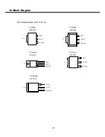
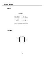
Страница 19: ...IC Block Diagram 19 LM4558 MP1482DS BS IN SW GND SS EN COMP FB 1 2 3 4 8 7 6 5 TOP VIEW ...
Страница 20: ...IC Block Diagram 20 MST6M20S LF ...
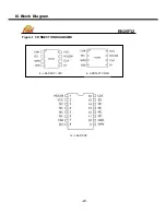
Страница 22: ...IC Block Diagram 22 EN25F32 Figure 1 CONNECTION DIAGRAMS 8 LEAD SOP DIP 8 CONTACT VDFN 16 LEAD SOP ...
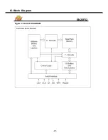
Страница 23: ...IC Block Diagram 23 EN25F32 Figure 2 BLOCK DIAGRAM ...
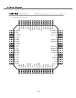
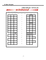
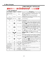
Страница 26: ...IC Block Diagram 26 TC90517FG Toshiba products specification Tentative CONFIDENTIAL 3 Pin Assignment Top view ...
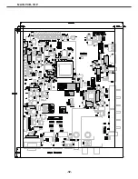
Страница 32: ...MAIN PCB TOP 32 ...
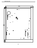
Страница 33: ...MAIN PCB BOT 33 ...

