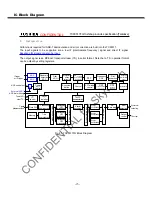
IC Block Diagram
-
3
0
-
PRELIMINARY W9751G6JB
5.
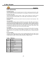
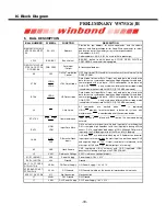
BALL DESCRIPTION
BALL NUMBER
SYMBOL
FUNCTION
DESCRIPTION
M8,M3,M7,N2,N8,N3
,N7,P2,P8,P3,M2,P7
,R2
A0−A12 Address
Provide the row address for active commands, and the column
address and Auto-precharge bit for Read/Write commands to select
one location out of the memory array in the respective bank.
Row address: A0−A12.
Column address: A0−A9. (A10 is used for Auto-precharge)
L2,L3 BA0−BA1
Bank
Select
BA0−BA1 define to which bank an ACTIVE, READ, WRITE or
PRECHARGE command is being applied.
G8,G2,H7,H3,H1,H9
,F1,F9,C8,C2,D7,D3,
D1,D9,B1,B9
DQ0−DQ15
Data Input
/ Output
Bi-directional data bus.
K9 ODT
On Die Termination
Control
ODT (registered HIGH) enables termination resistance internal to the
DDR2 SDRAM.
F7,E8
LDQS,
LDQS
LOW Data Strobe
Data Strobe for Lower Byte: Output with read data, input with write
data for source synchronous operation. Edge-aligned with read data,
center-aligned with write data.
LDQS corresponds to the data on
DQ0−DQ7. LDQS
is only used when differential data strobe mode
is enabled via the control bit at EMR (1)[A10 EMRS command].
B7,A8
UDQS,
UP Data Strobe
Data Strobe for Upper Byte: Output with read data, input with write
data for source synchronous operation. Edge-aligned with read data,
center-aligned with write data.
UDQS corresponds to the data on
DQ8−DQ15.
is only used when differential data strobe mode
is enabled via the control bit at EMR (1)[A10 EMRS command].
L8
Chip Select
All commands are masked when
is
registered
HIGH
.
provides for external bank selection on systems with
multiple ranks.
is considered part of the command code.
K7,L7,K3
RAS , CAS
Command Inputs
RAS , CAS and
(along with
) define the command being
entered.
B3,F3
UDM
LDM
Input Data Mask
DM is an input mask signal for write data. Input data is masked when
DM is sampled high coincident with that input data during a Write
access. DM is sampled on both edges of DQS. Although DM pins are
input only, the DM loading matches the DQ and DQS loading.
J8,K8
CLK,
CLK
Differential Clock
Inputs
CLK and CLK are differential clock inputs. All address and control
input signals are sampled on the crossing of the positive edge of CLK
and negative edge of CLK . Output (read) data is referenced to the
crossings of CLK and CLK (both directions of crossing).
K2 CKE
Clock
Enable
CKE (registered HIGH) activates and CKE (registered LOW)
deactivates clocking circuitry on the DDR2 SDRAM.
J2 V
REF
Reference
Voltage
V
REF
is reference voltage for inputs.
A1,E1,J9,M9,R1 V
DD
Power
Supply
Power Supply: 1.8V
±
0.1V.
A3,E3,J3,N1,P9 V
SS
Ground
Ground.
A9,C1,C3,C7,C9,E9,
G1,G3,G7,G9
V
DDQ
DQ Power Supply
DQ Power Supply: 1.8V
±
0.1V.
A7,B2,B8,D2,D8,E7,
F2,F8,H2,H8
V
SSQ
DQ Ground
DQ Ground. Isolated on the device for improved noise immunity.
A2,E2,L1,R3,R7,R8
NC
No Connection
No connection.
J7 V
SSDL
DLL Ground
DLL Ground.
J1 V
DDL
DLL Power Supply
DLL Power Supply: 1.8V
±
0.1V.
Содержание 8M29B
Страница 3: ... 3 LCD 8M29B chassis ...
Страница 5: ...For 42LED For 42LED 5 8 8 10 15 9800 12500 12500 266 276 9800 280 290 6500 313 329 ...
Страница 6: ...40 40 3 2 1 4 2 50 0 5 80 40 12000 6 24 6 ...
Страница 8: ... 8 4 ...
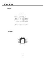
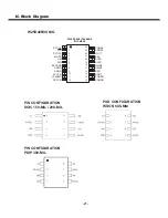
Страница 19: ...IC Block Diagram 19 LM4558 MP1482DS BS IN SW GND SS EN COMP FB 1 2 3 4 8 7 6 5 TOP VIEW ...
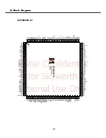
Страница 20: ...IC Block Diagram 20 MST6M20S LF ...
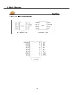
Страница 22: ...IC Block Diagram 22 EN25F32 Figure 1 CONNECTION DIAGRAMS 8 LEAD SOP DIP 8 CONTACT VDFN 16 LEAD SOP ...
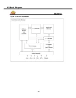
Страница 23: ...IC Block Diagram 23 EN25F32 Figure 2 BLOCK DIAGRAM ...
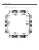
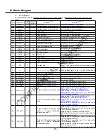
Страница 26: ...IC Block Diagram 26 TC90517FG Toshiba products specification Tentative CONFIDENTIAL 3 Pin Assignment Top view ...
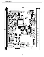
Страница 32: ...MAIN PCB TOP 32 ...
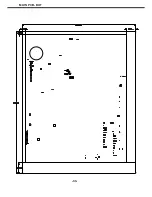
Страница 33: ...MAIN PCB BOT 33 ...

