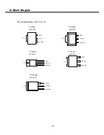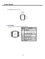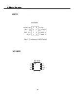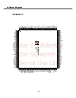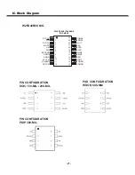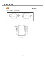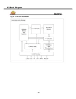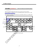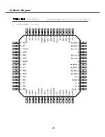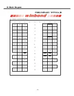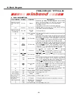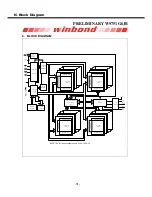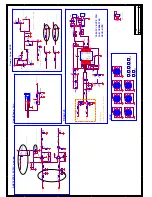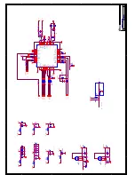
IC Block Diagram
-27-
IF signal (differential positive side)
4.
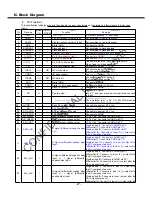
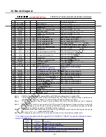
Pin Functions
This specification indicates pins and their signals in upper case letters and registers and their signals in lower case
letters
.
Pin
Pin name
(Note4)
I/O
(Note5,7)
PU/PD
Function
(Note 3)
s
k
r
a
m
e
R
(Note 2 and 6)
1
TSMD
0
I
-
Shut down
0: Normal operation
1: Shut down
2
XSEL1
I
-
Crystal frequency division ratio 1
Set according to crystal frequency.
3
XSEL0
I
-
Crystal frequency division ratio 0
Set according to crystal frequency.
4
VSS
-
-
Digital GND
Connects to DGND.
5
SLADRS1
I/O
-
Slave address 1
Set according to slave address.
6
SLADRS0
I/O
-
Slave address 0
Set according to slave address.
7
AGCI
I
-
External AGC input
Connects to DGND when not used.
8
S_INFO
I
-
Pin for pre-shipment test
Connects to DGND.
9
AGCCNTI
I/O
PD
IF_AGC control output
Connects to
tuner IF
_
AGC control input pin
.
1
0
AGCCNTR
I/O
PD
RF_AGC control output
Connects to tuner RF_AGC control input pin.
Open, fixed to L when not used.
11
CKI
I
-
Pin for pre-shipment test
Connects to DGND.
12
TNSCL
I/O
OD
I2C clock output
Connects to tuner I2C clock pin.
(Pull-up performed outside IC.)
13
VDDS
-
-
I/O power supply
Con
nects to d3
.
3 V typ
.
14
TNSDA
I/O
OD
I2C data I/O
Connects to tuner I2C data pin.
(Pull-up performed outside IC.)
15
VSS
-
-
Digital GND
Connects to DGND.
16
VDDC
-
-
D1.2 V power supply
Connects to d1.2 V typ.
17
PLLVSS
-
-
Clock PLL GND
Connects to AGND.
18
XO
O
-
Crystal output
Connects to crystal.
ixosl="1" and open when an external reference clock
is input.
19
XI
I
-
Crystal or reference clock input
Connects to crystal
.
The amplitude (p-p) is 0.5 V to PLLVDD when an
external reference clock is input
.
20
PLLVDD
-
-
Clock PLL power supply
Connects to 2.5 V typ.
21
FIL
O
-
PLL filter output
Connects to AGND via 15
00
pF
.
22
AD_AVDD
-
-
ADC analog power supply
Connects to 2.5 V typ.
23
AD_AVSS
-
-
ADC analog GND
Connects to AGND.
24
AD_VREFP
-
-
ADC reference voltage output
+1.75 V typ. Connects to AGND via PC.
25
AD_VREFN
-
-
ADC reference voltage output
+0.75 V typ. Connects to AGND via PC.
26
AD_VREF
-
-
ADC reference voltage output
+1.25 V typ. Connects to AGND via PC.
27
ADQ_AIN
I
-
Q signal (differential negative side)
input
Single-ended IF: Connects to AGND via PC.
Differential IF: Connects to AGND via PC.
Single-ended IQ: Connects to AGND via PC.
Differential IQ: Connects to tuner Q (-) output after
the DC component was cut.
28
ADQ_AIP
I
-
Q signal (differential positive side)
input
Single-ended IF: Connects to AGND via PC.
Differential IF: Connects to AGND via PC.
Single-ended IQ: Connects to tuner Q output after
the DC component was cut.
Differential IQ: Connects to tuner Q (+) output after
the DC component was cut.
29
ADI_AIN
I
-
IF signal (differential negative side)
input
or
I
signal
(differential
negative side) input
Single-ended IF: Connects to AGND via PC.
Differential IF: Connects to tuner IF (-) output after
the DC component was cut.
Single-ended IQ: Connects to AGND via PC.
Differential IQ: Connects to tuner I (-) output after the
DC component was cut.
30
ADI_AIP
I
-
input
or
I
signal
(differential
positive side) input
Single-ended IF: Connects to tuner IF output after
the DC component was cut.
Differential IF: Connects to tuner IF (+) output after
the DC component was cut.
Single-ended IQ: Connects to tuner I output after the
DC component was cut.
Differential IQ: Connects to tuner I (+) output after the
Содержание 8M29B
Страница 3: ... 3 LCD 8M29B chassis ...
Страница 5: ...For 42LED For 42LED 5 8 8 10 15 9800 12500 12500 266 276 9800 280 290 6500 313 329 ...
Страница 6: ...40 40 3 2 1 4 2 50 0 5 80 40 12000 6 24 6 ...
Страница 8: ... 8 4 ...
Страница 19: ...IC Block Diagram 19 LM4558 MP1482DS BS IN SW GND SS EN COMP FB 1 2 3 4 8 7 6 5 TOP VIEW ...
Страница 20: ...IC Block Diagram 20 MST6M20S LF ...
Страница 22: ...IC Block Diagram 22 EN25F32 Figure 1 CONNECTION DIAGRAMS 8 LEAD SOP DIP 8 CONTACT VDFN 16 LEAD SOP ...
Страница 23: ...IC Block Diagram 23 EN25F32 Figure 2 BLOCK DIAGRAM ...
Страница 26: ...IC Block Diagram 26 TC90517FG Toshiba products specification Tentative CONFIDENTIAL 3 Pin Assignment Top view ...
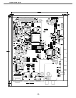
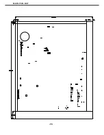
Страница 32: ...MAIN PCB TOP 32 ...
Страница 33: ...MAIN PCB BOT 33 ...

