Semiconductor Group
6-19
1999-04-01
On-Chip Peripheral Components
C541U
6.2.1.2
Mode 0
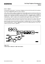
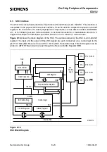
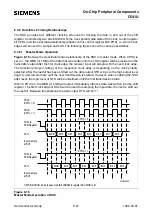
Putting either timer/counter 0,1 into mode 0 configures it as an 8-bit timer/counter with a divide-by-
32 prescaler. Figure 6-10 shows the mode 0 operation.
In this mode, the timer register is configured as a 13-bit register. As the count rolls over from all 1’s
to all 0’s, it sets the timer overflow flag TF0. The overflow flag TF0 then can be used to request an
interrupt. The counted input is enabled to the timer when TR0 = 1 and either Gate = 0 or INT0 = 1
(setting Gate = 1 allows the timer to be controlled by external input INT0, to facilitate pulse width
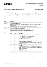
measurements). TR0 is a control bit in the special function register TCON; Gate is in TMOD.
The 13-bit register consists of all 8 bits of TH0 and the lower 5 bits of TL0. The upper 3 bits of TL0
are indeterminate and should be ignored. Setting the run flag (TR0) does not clear the registers.
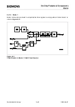
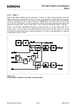
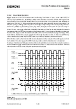
Mode 0 operation is the same for timer 0 as for timer 1. Substitute TR0, TF0, TH0, TL0 and INT0 for
the corresponding timer 1 signals in figure 6-10. There are two different gate bits, one for timer 1
(TMOD.7) and one for timer 0 (TMOD.3).
Figure 6-10
Timer/Counter 0, Mode 0: 13-Bit Timer/Counter
Содержание C541U
Страница 1: ... 8 LW 026 0LFURFRQWUROOHU 8VHU V 0DQXDO http www siem ens d Sem iconductor ...
Страница 7: ......
Страница 21: ...Semiconductor Group 2 6 1997 10 01 Fundamental Structure C541U ...
Страница 37: ...Semiconductor Group 4 6 1997 10 01 External Bus Interface C541U ...
Страница 133: ...Semiconductor Group 6 88 1999 04 01 On Chip Peripheral Components C541U ...
Страница 163: ...Semiconductor Group 8 8 1997 10 01 Fail Safe Mechanisms C541U ...
Страница 185: ...Semiconductor Group 10 14 1997 10 01 OTP Memory Operation C541U ...
Страница 192: ...Semiconductor Group 12 7 Index C541U ...


