


– 41 –
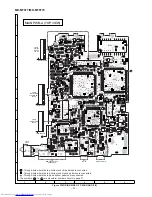
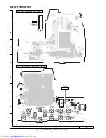
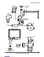
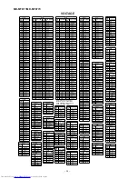
MD-MT877/MD-MT877C
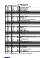
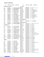
FUNCTION TABLE OF IC
1
PE5
SYRS
Output
System LSI register selection output.
2
PE6
_SYRD
Output
System LSI read enable output.
3
PE7
_SYWR
Output
System LSI write enable output.
4-11
PD0-PD7
SYD0-SYD7
Input/Output
System LSI parallel data bus.
12
CVCC
CVCC
Input
Power supply of internal voltage drop circuit.
13
PC0
PCLAT
Output
Record audio IC data latch output.
14
Vss
VSS
—
Ground potential.
15
PC1
_MCPGI
Input
Microphone plug insertion detection input.
16
PC2
_INPGI
Input
Line/digital plug insertion detection.
17
PC3
INPGCK
Input
Line/digital plug type detection.
18
PC4
RCPCNT
Input/Output
Record circuit power control output.
19*
PC5
TEST1
Input
Test mode setting input 1.
20*
PC6
TEST0
Input
Test mode setting input 0.
21
PC7
JPNP
Input
Kana conversion/Kana input existence/nonexistence discrimination.
22
PB0
OPICGA
Output
P.U detection sensitivity switching output.
23
PB1
RFRCNT
Output
RF_LSI power supply ON/OFF control output.
24
TIOCC3
BUZOUT
Output
Beep sound pulse output.
25
PB3
SGAIN
Output
RF amp gain pllarity switching output.
26
PB4
DISCP
Output
RF amp TE polarity switching output.
27*
TIOCB4
MCMON
Output
Internal operation status monitor.
28
PB6
RACLK
Output
Audio IC data clock output.
29
PB7
RADAT
Output
Audio IC serial data output.
30
PA0
CHGCNT
Output
Charge control.
31
TxD2
DSPDAT
Output
Unit indication data output.
32
PA2
DSPSTB
Output
Unit display strobe output.
33
SCK2
DSPSCK
Output
Unit indication data clock output.
34
P10
PBOPON
Output
Audio IC output stage control output.
35*
P11
P11
Output
Reserve
36
P12/TCLKA
CIN
Input
Track cross signal/focus drive detection.
37
TCLKB
SPIN
Input
Spindle motor FG pulse detection input.
38
IRQ0
_DINT
Input
System LSI interruption.
39
P15
DISCPR
Input
Disc record inhibition switch input.
40
IRQ1
ARQD
Input
Disk cap opens and closes detection/it is started and required.
41*
P17
P17
Output
Reserve
42
AVSS
AVSS
—
A/D and D/A converter ground potential.
43
DA1
LDVAR
Output
P.U. laser power setting output.
44*
DA0
PA0
Output
Reserve
45
AN7
RKCNG
Input
Remote control button operation detection input.
46
AN6
TEMP
Input
Ambient temperature detection input.
47
AN5
HKEY2
Input
Unit button operation detection input 2.
48
AN4
HKEY1
Input
Unit button operation detection input 1.
49
AN3
RKEY
Input
Remote control button operation detection input.
50
AN2
STDCK
Input
Lithium battery voltage detection input.
51
AN1
PLVDCI
Input
DC IN voltage detection input.
52
AN0
PLVBAT
Input
DC voltage detection input.
53
Vref
VREF
—
A/D and D/A converter reference voltage.
54
AVCC
AVCC
Input
A/D and D/A converter positive power supply.
55
MD0
MD0
Input
Operation mode selection input 0.
56
MD1
MD1
Input
Operation mode selection input 1.
57*
OSC2
OSC2
—
Sub clock (not used).
IC401 RH-iX0419AWZZ :System Microcomputer (IX0419AW) (1/2)
Pin No.
Function
Port Name
Terminal Name Input/Output
In this unit, the terminal with asterisk mark (*) is open terminal which is not connected to the outside.
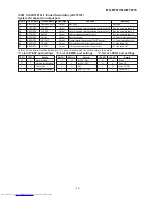
Содержание MD-MT877
Страница 44: ... 44 MD MT877 MD MT877C M E M O ...
Страница 54: ... M E M O MD MT877 MD MT877C 9 ...
Страница 55: ... M E M O MD MT877 MD MT877C 10 ...


