background image

CHAPTER 2. CONNECTION, ADJUSTMENT, OPERATION, AND FUNCTIONS

[1] CONNECTION, POWER ON/OFF

CONNECTING THE MONITOR TO A POWER SOURCE

Use only the AC adapter supplied.

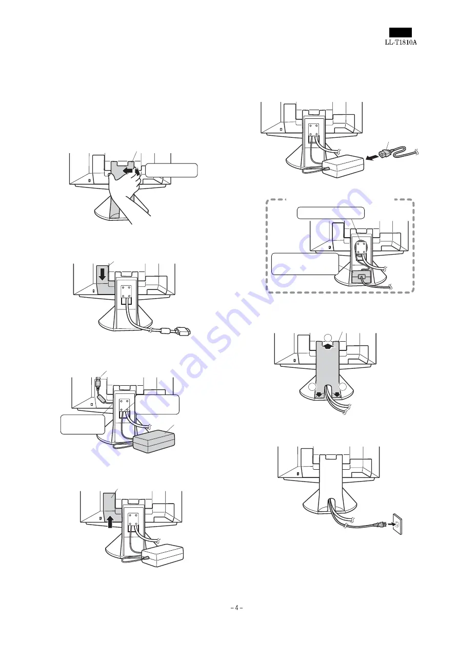
1. Remove the stand cover.

2. Remove the cover.

3. Connect the AC adapter to the monitor’s power terminal.

4. Replace cover.

5. Connect power cord to AC adapter.

6. Replace stand cover.

7. Place power plug into AC outlet.

(Rear View)

Stand cover

Lift one side

Cover

Power terminal

Place cord
on hook

Run cord
through hole.

AC adapter

Cover

Power cord

Fitting the AC adapter inside the stand

Wind the cord

Place adapter
inside stand cavity.

2

1

1

Stand cover

Содержание LL-T1810A

Страница 1: ...5 CHAPTER 7 PARTS LAYOUT 37 CONTENTS Parts marked with are important for maintaining the safety of the set Be sure to replace these parts with specified ones for maintaining the safety and performance of the set SHARP CORPORATION This document has been published to be used for after sales service only The contents are subject to change without notice SERVICE MANUAL ...

Страница 2: ...77 million colors 8 bit Dot pitch 0 2805 H 0 2805 V mm Brightness max 200cd m2 Contrast ratio 350 1 Angle of visibility Left right 150 Up down 150 Screen display size Horizontal 359 mm x Vertical 287 2 mm Video signal Analog RGB 0 7p p 75Ω Sync signal Separate Sync TTL level Sync on Green Composite Sync TTL level Frequencies Refer to relevant signal timing next page Automatic screen adjustment opt...

Страница 3: ... monitor is based on VESA DPMS Display Power Manage ment Signaling To activate the monitor s Power Management function both the video card and the computer must conform to the VESA DPMS standard DPMS mode Screen Power consumption H sync V sync ON Display on 54W Yes Yes STANDBY Display off Less than 4 5W No Yes SUSPEND Yes No OFFSTATE No No DDC Plug Play This monitor supports the VESA DDC Display D...

Страница 4: ...nction Ventilation openings Power terminal Remove the cover to see the power terminal The AC adapter is connected here INPUT 2 terminal and USB port Remove the cover to view the computer input terminal INPUT 2 and USB port INPUT 2 terminal A second computer can be connected here USB port Downstream A USB device can be connected here USB port Upstream A USB ready computer or self powered USB hub ca...

Страница 5: ...er 3 Connect the AC adapter to the monitor s power terminal 4 Replace cover 5 Connect power cord to AC adapter 6 Replace stand cover 7 Place power plug into AC outlet Rear View Stand cover Lift one side Cover Power terminal Place cord on hook Run cord through hole AC adapter Cover Power cord Fitting the AC adapter inside the stand Wind the cord Place adapter inside stand cavity 2 1 1 Stand cover ...

Страница 6: ...ure that the shape of the USB cable connector is correct For information regarding the USB function such as set up please refer to the operation manual of the computer to be connected Some devices may not be able to be activated To ascertain a certain device s USB compatibility please contact the manufacturer of the device 1 Remove the cover 2 Connect the USB cable 3 Replace the cover TURNING THE ...

Страница 7: ...on Arms or stands able to be used Attachments must satisfy the following Compatible with the VESA standard Have a gap of at least 100 mm x 100 mm between the screw holes on the section to be attached Not be likely to fall off or break off after being attached to the monitor How to attach the arm or stand Note While following these instructions please also refer to the in stallation instructions in...

Страница 8: ...tton are disabled Choosing a message language Messages displayed on the screen and OSD Menu contents can be changed to the following languages Dutch English French German Spanish Italian Swedish 1 Turn off the monitor 2 Pressing the and buttons simultaneously press the power button i e turn the power on The Language Selection Menu LANGUAGE will be displayed on the screen 3 Use the SELECT button to...

Страница 9: ... the BRIGHT bar will appear 2 Adjust by pressing the button darker or button lighter The BRIGHT bar automatically disappears approximately 3 seconds after the last command MANUAL SCREEN ADJUSTMENT Fine adjustments can be made using the On Screen Display OSD Menu provided MENU 1 ADJUSTMENT CLOCK PHASE H POS horizontal positioning and V POS vertical positioning MENU 2 GAIN CONTROL BRIGHT brightness ...

Страница 10: ...setting values remain unchanged BRIGHT brightness Total screen brightness can be adjusted while watching the color pattern buttons CONT Contrast While watching the color pattern adjustments can be made so that all graduations appear buttons MENU 3 WHITE BALANCE WHITE BALANCE can be adjusted as necessary As adjustments are made before shipment there is no real necessity for further al teration Note...

Страница 11: ...z 60 0Hz 65 0MHz 56 5kHz 70 0Hz 75 0MHz 60 0kHz 75 0Hz 78 75MHz 68 7kHz 85 0Hz 94 5MHz 1152 x 864 67 5kHz 75 0Hz 108 0MHz 1280 x 960 60 0kHz 60 0Hz 108 0MHz 1280 x 1024 64 0kHz 60 0Hz 108 0MHz 80 0kHz 75 0Hz 135 0MHz US text 720 x 400 31 5MHz 70 0Hz 28 3MHz Display mode Hsync Vsync Dot frequency Power Macintosh series 640 x 480 35 0kHz 66 7Hz 30 2MHz 832 x 624 49 7kHz 74 6Hz 57 3MHz 1024 x 768 60 ...

Страница 12: ...er supply line and power supply circuit around fuse DC jack board Test terminal TP4 shows DC 5V Check DC 5V power supply line MVCC and power supply circuit around the IC4 IC34 No 19 pins signal input is at H level DC 5V Check RESET circuit around IC29 IC34 No 22 pins signal input is normal See waveform diagram 1 Check clock circuit around IC34 and X1 IC34 No 55 pins signal output is at H level DC ...

Страница 13: ...12V Check DC 12V power supply line and power supply circuit around fuses F1 and F2 No 4 pins of CN1 and CN2 show DC 5V Check inverter board unit and cable IC34 No 55 pins signal output is at the H level DC 5V Check microprocessor control circuit around IC29 and IC34 Test terminal TP1 shows DC 11V Check DC 11V power supply line 11V and power supply circuit around IC1 IC34 No 54 pins signal output i...

Страница 14: ...ntire screen of LCD display remains black IC34 No 56 pins signal output is at the H level DC 5V Check microprocessor control circuit around IC29 and IC34 No Yes Yes No Yes No No Check LCD control signal circuit around IC26 and IC27 LCD screen size is abnormal Adjustment items of ADJUSTMENT and MODE SELECT are set correctly Adjust and set screen according to the LCD screen setting procedure Signal ...

Страница 15: ...o switch circuit around IC14 Analog color signal outputs of No 15 pins of IC 401 IC402 and IC403 are normal See waveform diagram 12 Check video amplifier circuit around IC401 IC402 IC403 and IC28 Digital color signal output of IC 23 is normal See waveform diagram 13 Check AD converter circuit around IC23 Digital color signal input and output of IC 27 is correct See waveform diagrams 14 and 15 Chec...

Страница 16: ...romatic gradation patterns 13 52 59 pins and 62 69 pins of R of the IC23 32 39 pins and 42 49 pins of the G of the IC23 12 19 pins and 22 29 pins of B of the IC23 A D OUT DATA Monochrome pattern at every 2 lines 14 242 259 pins 262 268 pins 276 278 pins 281 292 pins and 295 302 pins of the IC27 ASIC IN DATA Monochrome pattern at every 2 lines 15 156 163 pins 166 174 pins 177 183 pins 191 204 pins ...

Страница 17: ...Display Screen arbitrary WAVE FORM 3 HSYNC 8 pin 17 pin of the IC14 Frequency 80kHz Display Screen arbitrary WAVE FORM 4 MPU VSY 6 pin of the IC34 Frequency 75Hz Display Screen arbitrary WAVE FORM 5 MPU HSY 7 pin of the IC34 Frequency 80kHz Display Screen arbitrary WAVE FORM 6 LCD CLKA CLKB FL4 FL3 Frequency 50MHz Display Screen arbitrary ...

Страница 18: ...in of the IC23 Frequency 65MHz Display Screen arbitrary WAVE FORM 10 SOGOUT 25 pin of the IC14 Display Screen 16 monochromatic gradation patterns WAVE FORM 11 VSwitch RGB OUT 27 pin 30 pin and 35 pin of the IC14 Display Screen 16 monochromatic gradation patterns WAVE FORM 12 VAmp RGB OUT 16 pin of the IC401 IC402 and IC403 Display Screen 16 monochromatic gradation patterns ...

Страница 19: ...reen Monochrome pattern at every 2 lines WAVE FORM 15 ASIC OUT DATA 156 163 pins 166 174 pins 177 183 pins 191 204 pins 207 216 pins of the IC27 Display Screen Monochrome pattern at every 2 lines WAVE FORM 16 ASIC IN OUT DATA 1 3 4 6 7 9 10 12 13 17 18 20 21 60 61 63 64 68 69 71 72 74 75 77 78 80 81 83 84 97 98 100 pins of IC8 IC9 and IC10 Display Screen Monochrome pattern at every 2 lines ...

Страница 20: ...B signal input 2 Synchronizing separator 3 A D converter and PLL circuit 4 ASIC circuit 5 SGRAM circuit 6 Microprocessor 7 LCD output connector circuit 8 Power supply circuit DC jack board Sheet No Description 1 DC jack and fuse circuit LED SW board Sheet No Description 1 LED and switch circuit D sub board Sheet No Description 1 D Sub connector and DDC circuit ...

Страница 21: ...IC terminal diagram 1 3 ...

Страница 22: ...IC terminal diagram 2 3 ...

Страница 23: ...IC terminal diagram 3 3 ...

Страница 24: ...4W 5025 1W Type Resistance Carbon tact film resistance Volume resistance 2 Capacitor indications Capacitor Aluminium electrolytic capacitor Unit F F PF PF Rated voltage 10V 10V 16V 16V 25V 25V 35V 35V 50V 50V Ceramic capacitor Unit F F PF PF Temperature characteristic No indication 30 80 B 10 CH 0 Rated voltage No indication 50V 16V 16V 25V 25V Type Capacitor Ceramic capacitor Non polarity alumini...

Страница 25: ...CK SOUT OSD R OSD G OSD B OSD BK OSD HS OSD VS OSD CK S_OSC2 IC31 OSD M35072 IC33 Buffer TC74VHCT125 GA CS1 GA CS2 SCK SOUT 8 8 8 8 8 8 IC27 Controller IX0033UP I23 A D Converter AD9483 SIN DSYNC AD CLK R2O7 0 R1O7 0 G2O7 0 G1O7 0 B2O7 0 B1O7 0 SGA10 0 32 32 32 11 GDQ31 0 BDQ31 0 RDQ31 0 IC10 SGRAM MB81G163222 80 IC9 SGRAM MB81G163222 80 IC8 SGRAM MB81G163222 80 SG CLK CKE WE CS RAS CAS DSF DQM3 0...

Страница 26: ...440 47uF 16V WX C420 10uF 16V WX R132 62J C134 100uF 16V WX C106 100uF 16V WX R411 470J R425 100D TP53 C422 1uF 50V WP C135 0 01uF B FB6 BLM11B750S D401 EMPTY R418 100J TP61 C423 0 01uF B C137 100uF 16V WX R128 75D 2125 1 10W C402 3 3uF 35V WX C433 EMPTY TP62 C114 47uF 16V WX C424 47uF 16V WX C138 0 01uF B FB7 BLM11B750S C412 47uF 16V WX C434 3 3uF 35V WX TP63 C425 0 01uF B C115 47uF 16V WX C139 1...

Страница 27: ... 12 VCC 16 GND 8 R167 EMPTY C505 0 1uF IC22 PST572DMT VC 1 OUT 3 G 2 R181 510D R520 EMPTY R1608 R508 4 7kJ C165 EMPTY 4 7uF 16V WP C169 47uF 16V WX R180 1kD R166 56kD C168 0 1uF R195 4 7kJ C157 0 01uF B R193 100J X3 R182 EMPTY C156 EMPTY C1608 R192 Q6 EMPTY 2SC2712 R191 C164 4 7uF 16V WP x2 R165 EMPTY R1608 C167 0 1uF R179 4 7kJ R164 EMPTY R1608 R190 EMPTY R178 EMPTY R163 18kD R189 EMPTY C163 0 1u...

Страница 28: ...2 3 4 5 6 7 C209 R213 330J R198 EMPTY RA6 33J x4 x2 8 1 2 3 4 5 6 7 C210 0 1uF X12 R214 330J RA7 8 1 2 3 4 5 6 7 C212 0 1uF R215 330J RA8 33J x4 x2 8 1 2 3 4 5 6 7 C213 0 1uF R216 330J RA9 8 1 2 3 4 5 6 7 R219 0 R217 1 6kD RA10 8 1 2 3 4 5 6 7 C211 0 33uF B 3216 RA11 8 1 2 3 4 5 6 7 R200 0 R220 RA12 33J x4 x4 8 1 2 3 4 5 6 7 R201 0 R205 EMPTY R221 R199 EMPTY C181 47uF 16V WX R207 EMPTY R222 R210 R...

Страница 29: ...SD_CK 219 OSD_BLK 222 OSD_VS 220 OSD_HS 221 OSD_B 224 OSD_G 225 OSD_R VSS 226 253 254 255 256 257 258 259 261 262 263 264 265 274 266 267 269 272 270 271 268 276 277 278 280 281 282 283 284 285 286 287 288 289 290 291 294 293 292 295 296 297 298 299 300 301 302 273 VDD 54 DSF 51 SGA10 52 SGA9 53 SGA8 56 SGA7 57 SGA6 58 SGA5 59 SGA4 60 SGA3 61 VSS 43 VDD CCLK 75 SGA2 62 SGA1 63 SGA0 64 DQM3 VSS 65 ...

Страница 30: ...31 84 VSS 85 NC 86 NC 87 NC 88 NC 89 NC 90 NC 91 NC 92 NC 93 NC 94 NC 95 VDD 96 DQ0 97 DQ1 98 VSSQ 99 R85 R74 R65 R30 R48 C45 C66 R75 R66 R31 R49 C48 C67 R91 R67 R32 R50 C52 0 01uF B x5 R99 R92 R68 R33 C76 0 01uF B C44 IC10 MB81G163222 80 DQ3 1 VDDQ 2 DQ4 3 DQ5 4 VSSQ 5 DQ6 6 DQ7 7 VDDQ 8 DQ16 9 DQ17 10 VSSQ 11 DQ18 12 DQ19 13 VDDQ 14 VDD 15 VSS 16 DQ20 17 DQ21 18 VSSQ 19 DQ22 20 DQ23 21 VDDQ 22 D...

Страница 31: ...3 GND 2 C256 0 01uF B R335 6 8kJ C303 R323 R354 R365 EMPTY IC34 M38027E8FP VCC 57 VREF 58 AVSS 59 P6 7 AN7 60 P6 6 AN6 61 P6 5 AN5 62 P6 4 AN4 63 P6 3 AN3 64 P6 2 AN2 1 P6 1 AN1 2 P6 0 AN0 3 P5 7 INT3 4 P5 6 PWM 5 P5 5 CNTR1 6 P5 4 CNTR0 7 8 P5 2 SCLK2 9 P5 1 SOUT2 10 P5 0 SIN2 11 12 P4 6 SCLK1 13 P4 5 TXD 14 P4 4 RXD 15 P4 3 INT2 16 P4 2 INT1 17 CNVSS 18 RESET 19 P4 1 INT0 20 XIN 22 XOUT 23 VSS 2...

Страница 32: ...13 BD6 115 BD5 117 BD4 119 VCC 121 BD3 123 BD2 125 BD1 127 BD0 129 GND 131 BLON 133 GND 135 VDD 137 VDD 139 BA0 62 GND 64 DEA 66 VCC 68 CLKA 70 GND 72 RB7 74 RB6 76 RB5 78 RB4 80 VCC 82 RB3 84 RB2 86 RB1 88 RB0 90 GND 92 GB7 94 GB6 96 GB5 98 GB4 100 VCC 102 GB3 104 GB2 106 GB1 108 GB0 110 GND 112 BB7 114 BB6 116 BB5 118 BB4 120 VCC 122 BB3 124 BB2 126 BB1 128 BB0 130 GND 132 MODE 134 GND 136 VDD 1...

Страница 33: ...D 5 L8 CDRH127 47uH IC5 LTC1147 5 SHUTDOWN 6 VIN 1 P DRIVE 8 SENSE 5 SENSE 4 GND 7 CT 2 ITH 3 R5 0 C36 470uF 16V UR L5 CDR74B 100uH TP5 CN1 S5B PH SM3 TB 1 2 3 4 5 R10 1kD L6 CDR74B 100uH C26 0 1uF D3 RD5 1M B2 C283 0 33uF B 3216 TP31 F5 SSFC 0 5A C27 47uF 20V SN TP2 C284 0 1uF TP32 Q4 2SJ332 2 3 1 C7 330uF 25V UR R428 10kJ C30 330uF 25V UR L3 CDRH127 47uH TP3 R427 10kJ C31 330uF 25V UR R15 RN1A2H...

Страница 34: ...DC JACK PWB 1 1 ...

Страница 35: ... 1 1 CN1 S9B ZR 3 4 1 2 3 4 5 6 7 8 9 SW5 SKHHAJ 1 4 2 3 SW4 SKHHAJ 1 4 2 3 SW3 SKHHAJ 1 4 2 3 SW2 SKHHAJ 1 4 2 3 SW1 SKHHAJ 1 4 2 3 SW6 SPPH210100 4 5 6 3 2 1 D1 L 3VEGW 3 2 1 INPUT RED POW SW SELECT GREEN MENU ...

Страница 36: ...D sub PWB 1 1 ...

Страница 37: ...USB PWB 1 1 ...

Страница 38: ...Main PWB front surface CHAPTER 7 PARTS LAYOUT Symbol PartsCod ...

Страница 39: ...Main PWB rear surface ...

Страница 40: ...oredinaretrievalsystem ortransmitted Inanyformorbyanymeans electronic mechanical photocopying recording orotherwise withoutpriorwrittenpermissionofthepublisher SHARP CORPORATION Digital Document Systems Group Quality Reliability Control Center Yamatokoriyama Nara 639 1186 Japan 2001 January Printed in Japan ...

Отзывы: