background image

− 16 −

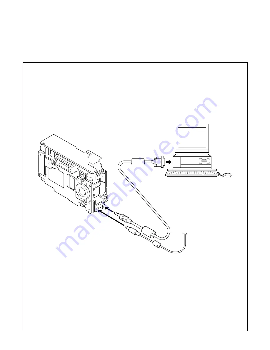
3-5. Connecting the camera to the computer

1. Turn off both camera and computer.
2. Locate the port cover on the side of the camera. Press on the arrows and slide the cover down to open it.
3. Line up the arrow on the cable connector with the notch on the camera's serial port. Insert the connector.
4. Locate a serial port on the back of your computer. You may have two serial ports labeled COM1 and COM2, or the ports may

be labeled with icons. If you have two serial ports available, use port 1 to connect your camera.

5. Line up the serial connector on the cable with one of the serial ports on your computer, and insert the connector.

6. Turn on the camera and your computer system.

AC adaptor

Serial cable

To COM1 or COM2 serial port

Содержание VPC-X360

Страница 1: ... to product safety Should any component designated by a symbol need to be replaced use only the part designated in the Parts List Do not deviate from the resistance wattage and voltage ratings shown CAUTION Danger of explosion if battery is incorrectly replaced Replace only with the same or equivalent type recommended by the manufacturer Discard used batteries according to the manufacturer s instr...

Страница 2: ...on DC 15 V When sensor read out 1 OUTLINE OF CIRCUIT DESCRIPTION 1 1 CA 1 CIRCUIT DESCRIPTION 1 IC Configuration IC903 ICX204AK CCD imager IC902 74VHC04MTC H driver IC904 CXD1267AN V driver IC905 AD9802 CDS AGC A D converter 2 IC903 CCD Structure Interline type CCD image sensor Optical size 1 3 inch format Effective pixels 1034 H 779 V Pixels in total 1077 H 788 V Chip size 5 80 mm H 4 92 mm V Uni...

Страница 3: ...the XSUB signal which is output from Pin 165 of IC102 is used as the sweep pulse for the electronic shutter and the RG signal which is output from Pin 159 of IC102 is the reset gate clock 4 IC905 CDS AGC Circuit and A D converter The video signal which is output from the CCD is input to Pins 26 and 27 of IC905 There are S H blocks inside IC905 generated from the XSHP and XSHD pulses and it is here...

Страница 4: ...inal stage of the horizontal CCD are transferred to the floating diffusion as shown in Fig 1 5 RG is turned on by the timing in 1 and the floating diffusion is charged to the potential of PD The RG is turned off by the timing in 2 In this condition the floating diffusion is floated at high impedance The H1 potential becomes shallow by the timing in 3 and the electric charge now moves to the floati...

Страница 5: ...bit digital signals 1 8 8 bit A D circuit Audio The audio signals which were converted to digial form by the 8 bit A D circuit are temporarily to a sound buffer and then recorded in the SSFDC card During playback the 8 bit D A circuit converts these signals into analog audio signals 1 9 Sound buffer Audio memory 1 10 LCD driver The Y C signals which are input to the LCD driver are con verted to RG...

Страница 6: ...y as for EE the data is then sent to the SDRAM after which D A conversion is carried out inside the ASIC and then the data is sent to the LCD panel and displayed The LCD driver is converted Y C signals to RGB signals from ASIC and these RGB signals and the control signal which is output by the LCD driver are used to drive the LCD panel The RGB signals are 1H transposed so that no DC compo nent is ...

Страница 7: ...ined at the correct voltage set ting level 2 1 Short circuit protection circuit If output is short circuited for the length of time determined by the condenser which is connected to Pin 17 of IC501 all output is turned off The control signal P ON P A ON and LCD ON are recontrolled to restore output 3 Digital 3 3 V Power Output 3 3 V D is output Feedback for the 3 3 V D is provided to the switching...

Страница 8: ... current which is generated at the secondary side of T5401 is rectified to produce a high voltage direct current and is accumulated at electrolytic ca pacitor C5412 on the main circuit board 1 6 Voltage monitoring circuit This circuit is used to maintain the voltage accumulated at C5412 at a constance level After the charging voltage is divided and converted to a lower voltage by R5417 and R5419 i...

Страница 9: ... data output ASIC Serial communication clock output ASIC Connect to Vss Main clock oscillation terminal 4 MHz Main clock oscillation terminal Power supply terminal Sub clock oscillation terminal 32 768 kHz Sub clock oscillation terminal Reset input Battery OFF detection signal L OFF RS 232C RXD input terminal Serial communication request signal L Request Key matrix output 1 5 SY1 CIRCUIT DESCRIPTI...

Страница 10: ...circuits The 8 bit microprocessor reads the signals from each sensor element as input data and outputs this data to the camera circuits ASIC or to the LCD display device as operation mode setting data Fig 4 1 shows the internal commu nication between the 8 bit microprocessor and ASIC 3 Key Operaiton For details of the key operation refer to the instruction manual 8 bit microprocessor ASIC 32 bit C...

Страница 11: ...AVE Power save mode 4 MHz Main clock operation 32 kHz Sub clock operation 4 Power Supply Control The 8 bit microprocessor controls the power supply for the overall system The following is a description of how the power supply is turned on and off When the battery is attached a regulated 3 3 V voltage is normally input to the 8 bit microprocessor IC301 by IC303 so that clock counting and key scanni...

Страница 12: ...Cover battery 3 Back cabinet 1 Four screws 1 7 x 4 5 Cover jack 6 Screw 1 7 x 3 7 Cabinet top 8 Screw 1 7 x 3 9 Two screws 1 7 x 4 10 Holder SSFDC 11 Holder terminal 12 Five screws 1 7 x 3 13 Holder battery 1 Two screws 1 7 x 3 2 FPC 3 Three connectors 4 Connector 5 SY1 board 6 Screw 1 7 x 3 7 TB2 board 8 Screw 1 7 x 3 9 Unit control panel 10 Screw 1 7 x 3 11 TB1 board ...

Страница 13: ... 13 2 3 REMOVAL OF LENS VF AND PW1 BOARD 1 Two screws 1 7 x 3 2 Lens VF 3 Two screws 1 7 x 3 4 Connector 5 Connector 6 Three screws 1 7 x 3 7 Holder chassis PW1 8 Reflector 9 PW1 board ...

Страница 14: ...B2 board TB1 board PW1 board CA1 board CA2 board 1 FPC 2 LCD 3 Four screws 1 7 x 3 4 Connector 5 Screw 1 7 x 3 6 Two connectors 7 Two screws 1 7 x 3 8 Holder chassis CA2 9 CA2 board 10 Three screws 1 7 x 3 11 Holder chassis CA1 12 Two screws 1 7 x 6 13 Screw 1 7 x 4 14 CA2 board ...

Страница 15: ...s Windows 95 or 98 IBM R compatible PC with 486 or higher processor CD ROM drive 3 5 inch high density diskette drive Serial port with standard RS 232C interface 8 MB RAM Hard disk drive with at least 15 MB available VGA or SVGA monitor with at least 256 color display 2 Installing calibration software 1 Insert the calibration software installation diskette into your diskette drive 2 Open the explo...

Страница 16: ... serial port Insert the connector 4 Locate a serial port on the back of your computer You may have two serial ports labeled COM1 and COM2 or the ports may be labeled with icons If you have two serial ports available use port 1 to connect your camera 5 Line up the serial connector on the cable with one of the serial ports on your computer and insert the connector 6 Turn on the camera and your compu...

Страница 17: ...L Voltage Adjustment Adjustment method 1 Adjust with VR506 to 5 80 0 05 V 7 CCD Defect Detect Adjustment Adjustment method 1 Set the camera mode and turn on the power switch to open the lens cover 2 Double click on the DscCalV123b 3 Select CCD Defect on the LCD Test and click the Yes 4 After the adjustment is completed OK will display 5 Close the lens cover Measuring Point ADJ Location Measuring E...

Страница 18: ...infront of the lens 4 Turn the adjustment screw until the Siemens star which is 1 0 meters away is exactly in focus Check that the Siemens star which is 0 3 meters from the front of the lens is out of focus at this time 5 Project the Siemens star chart at a distance of 0 3 meters in front of lens Check that it is out of focus at normal mode and it is in focus at macro mode 6 This adjustment locati...

Страница 19: ...od 1 Adjust LCD B Bright so that the amplitude of the CL426 waveform is 0 2 V with respect to the CL424 VG wave form Note 10 2 LCD RGB Offset adjustment and 10 3 LCD Gain ad justment should always be carried out first CL424 waveform CL425 waveform VG VG 0 2 V 7 5 Vp p 0 3 V CL424 waveform CL424 waveform 4 0 Vp p 0 15 V 10 5 LCD Red Brightness Adjustment Adjusting method 1 Adjust LCD R Bright so th...

Страница 20: ...z OSCILLATION CHECK L1105 SD CLK 57 MHz OSCILLATION IC106 35 IC101 111 114 IC301 75 76 CHECK ASIC AND MEMORY PIN INCORRECT HANDSHAKING BETWEEN 8 BIT CPU AND RS 232C CHECK EACH INTERFACE PUSH SHUTTER BUTTON IC301 4 5 SCAN IN 0 1 PULSE INPUT CHECK S3029 D3064 R3021 R3022 IC301 70 71 P ON P A ON CHECK IC301 IC301 96 97 98 HIGH CHECK IC301 IC101 SERIAL COMMUNICATION IC301 75 77 87 CHECK IC301 R3001 R3...

Страница 21: ...J 15 636 055 5747 COVER JACK SR662 J 16 636 055 5853 HOLDER TERMINAL SR662 J 17 636 056 0956 DEC MONITOR SR662 E 18 636 055 9080 ASSY CABINET BACK SR662 J 19 636 055 5938 KNOB POWER SR662 J 20 636 057 0214 SPRING COMP RELEASE 662 J 21 636 055 9042 ASSY BUTTON SHUTTER 662 J 22 636 056 0932 CABINET TOP SR662 E 23 636 055 5990 SLIDE KNOB POWER SR662 J 24 636 055 6058 TERMINAL BATTERY A SR662J 25 636 ...

Страница 22: ... 055 4306 COMPL PWB TB 1 15 636 055 5815 HOLDER CHASSIS CA2 662 J 16 636 055 4276 COMPL PWB CA 2 EXCEPT VPC X360 16 636 056 6705 COMPL PWB CA 2 VPC X360 ONLY 17 636 055 4290 COMPL PWB PW 1 18 636 055 5822 HOLDER CHASSIS PW1 662 J 19 636 055 4313 COMPL PWB TB 2 20 636 055 8892 COMPL REFLECTOR 21 636 055 4283 COMPL PWB SY 1 22 636 055 5877 HOLDER VF SR662 J 23 645 023 4248 ASSY LENS VF 24 636 055 59...

Страница 23: ...7 645 014 8064 INDUCTOR 120 OHM L1708 645 020 2070 INDUCTOR 750 OHM L1709 645 020 2070 INDUCTOR 750 OHM L9001 645 001 4512 INDUCTOR 10U K L9010 645 020 1875 INDUCTOR 1500 OHM L9010 645 020 1882 INDUCTOR 1800 OHM CAPACITORS C1700 403 312 6805 CERAMIC 0 1U Z 16V C1702 403 332 9503 CERAMIC 1U M 6 3V C1703 403 311 4505 CERAMIC 1000P K 50V C1705 403 312 6003 CERAMIC 39P J 50V C1706 403 319 3005 CERAMIC...

Страница 24: ...K JA 1 16W R2023 401 226 1503 MT GLAZE 0 000 ZA 1 16W R2024 401 224 9006 MT GLAZE 10K JA 1 16W R2025 401 226 1503 MT GLAZE 0 000 ZA 1 16W R9010 401 267 3207 MT GLAZE 330 DC 1 16W R9011 401 262 1604 MT GLAZE 2 2K DC 1 16W R9012 401 224 9006 MT GLAZE 10K JA 1 16W R9013 401 037 5004 MT GLAZE 0 000 ZA 1 10W R9016 401 226 1503 MT GLAZE 0 000 ZA 1 16W R9018 401 224 9402 MT GLAZE 1 0M JA 1 16W R9019 401 ...

Страница 25: ...1 225 0309 MT GLAZE 33 JA 1 16W R1016 401 225 0309 MT GLAZE 33 JA 1 16W R1017 401 225 0309 MT GLAZE 33 JA 1 16W R1018 401 225 0309 MT GLAZE 33 JA 1 16W R1019 401 225 0309 MT GLAZE 33 JA 1 16W R1020 401 225 7902 MT GLAZE 220 JA 1 16W R1021 401 225 7902 MT GLAZE 220 JA 1 16W R1022 401 225 7902 MT GLAZE 220 JA 1 16W R1023 401 225 7902 MT GLAZE 220 JA 1 16W R1024 401 225 7902 MT GLAZE 220 JA 1 16W R10...

Страница 26: ...IODE MA141WK OR 407 106 1601 DEODE DCG015 D5410 407 151 4701 DIODE 1SS301 TE85L OR 407 130 4401 DIODE DAN202U OR 407 134 7408 DIODE MA141WK OR 407 106 1601 DEODE DCG015 VARIABLE RESISTORS VR501 645 028 2249 VR SEMI 3 3K S VR502 645 028 2201 VR SEMI 2 2K S VR503 645 028 2201 VR SEMI 2 2K S VR504 645 019 5143 VR SEMI 1K S VR505 645 019 5143 VR SEMI 1K S VR506 645 019 5143 VR SEMI 1K S INDUCTORS L500...

Страница 27: ... JA 1 16W R5061 401 274 9704 MT GLAZE 24K DC 1 16W R5062 401 224 9402 MT GLAZE 1 0M JA 1 16W R5063 401 224 9402 MT GLAZE 1 0M JA 1 16W R5064 401 263 1702 MT GLAZE 1 2K DC 1 16W R5065 401 258 9102 MT GLAZE 5 6K DC 1 16W R5066 401 258 9300 MT GLAZE 220K DC 1 16W R5067 401 258 0406 MT GLAZE 120K DC 1 16W R5068 401 224 9402 MT GLAZE 1 0M JA 1 16W R5069 401 262 2304 MT GLAZE 1 0K DC 1 16W R5070 401 258...

Страница 28: ...4 8900 MT GLAZE 100K JA 1 16W R3052 401 224 8900 MT GLAZE 100K JA 1 16W R3053 401 224 9303 MT GLAZE 1K JA 1 16W R3056 401 224 9303 MT GLAZE 1K JA 1 16W R3101 401 224 9501 MT GLAZE 2 2K JA 1 16W R3102 401 224 9501 MT GLAZE 2 2K JA 1 16W R3103 401 224 9006 MT GLAZE 10K JA 1 16W R3104 401 224 8801 MT GLAZE 100 JA 1 16W R3105 401 225 1207 MT GLAZE 4 7K JA 1 16W R3106 401 224 9303 MT GLAZE 1K JA 1 16W ...

Страница 29: ...OVERALL WIRING ...

Отзывы: