background image

MultiMediaCard Product Manual

SanDisk MultiMediaCard Product Manual Rev. 2 © 2000 SANDISK CORPORATION

40

5.2.2

Operating Voltage Range Validation

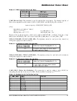
The MultiMediaCard standard requires  that a l l
MultiMediaCards will  be able to establish
communication with the host  using any  operating
voltage between V

DD

-min and


V

DD

-max. However,

during  data transfer minimum  and  maximum
values for


V

DD 

are defined in the card  specific

data register (CSD)  and may not cover the  whole
range. MultiMediaCard hosts are expected to read
the  card’s CSD register  and  select proper


V

D D

values or reject the card.

MultiMediaCards that store  the  CID  and CSD
data in the payload memory can communicate this
information only under 

data-transfer V

D D

conditions. This  means if host  and  card  have non
compatible


V

DD 

ranges, the card will not be able to

complete the identification cycle, nor to send CSD
data.

SEND_OP_COND (CMD1) is designed to provide
MultiMediaCard  hosts  with a mechanism to
identify  and reject cards which do not  match the
host’s desired V

DD 

range. This is accomplished by

the host sending the required


V

DD 

voltage  window

as the  operand of this 

command.

MultiMediaCards which  can not perform  data
transfer in the  specified  range  must  discard
themselves from further bus operations and go into
Inactive State.  All  other MultiMediaCards will
respond  concurrently  (same method as card
identification)  sending back their


V

DD

 range. The

wired-or result of the  response  will  show a l l
voltage  ranges  which  some of the  cards do not
support.

By omitting the voltage range in the  command,
the host can query the MultiMediaCard stack and
determine if there are any  non  compatibilities
before sending out-of-range cards into the  Inactive
State.  Bus query should be used if the host can
select a common voltage  range or wants to notify
the application of non usable cards in the stack.

The busy bit in the CMD1 response can be used by a
card to tell the  host that it is still working on its
power-up/reset  procedure  (e.g.  downloading the
register information from memory field) and is not
ready yet for communication. In this  case the  host
must repeat CMD1 until the busy bit is cleared.

During  the  initialization  procedure,  the host is
not allowed to change the OCR values. Changes in

the  OCR  content  will be ignored by the
MultiMediaCard. If there is a real change in the
operating  conditions the host must  reset the card
stack  (using  CMD0)  and begin the  initialization
procedure once more.

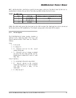
GO_INACTIVE_STATE (CMD15) can also be used
to send an addressed  MultiMediaCard  into the
Inactive State. This  command is used when the
host  explicitly  wants to deactivate a card  (e.g.
host is changing V

DD 

into a range which is known

to be not supported by this card).

5.2.3

Card Identification Process

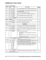
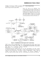
The host starts the card  identification  process in
open-drain  mode  with the identification clock
rate f

OD

. The open drain driver stages on the  CMD

line allow parallel  card operation  during  card
identification.

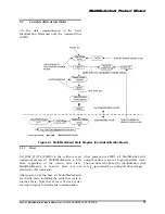
After the bus is activated  and a valid operation
condition is obtained, the host  then  asks all  cards
for their  unique card identification (CID) number
with the broadcast  command  ALL_SEND_CID
(CMD2). All remaining unidentified  cards  (i.e.
those which are in Ready  State)  simultaneously
start  sending  their  CID  numbers  serially,  while
bit-wise  monitoring  their  outgoing  bit  stream.
Those cards, whose outgoing CID bits do not match
the corresponding bits on the  command line in any
one of the bit periods, stop  sending  their CID
immediately  and  must  wait  for  the  next
identification  cycle (cards stay  in the  Ready
State).  Since CID numbers  are  unique  for  each
MultiMediaCard, there should be only one  card
which  successfully  sends  its full CID-number to
the host. This card then goes  into  Identification
State. 

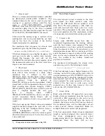
The host issues 

CMD3,

(SET_RELATIVE_ADDR) to assign  this  card a
relative  address  (RCA), which is shorter than
CID and which will be used to address the  card in
future 

data transfer mode 

communication

(typically  with a higher clock  rate than f

OD

).

Once the RCA is received the card transfers  to the
Stand-by  State  and  does not react to further
identification  cycles. The MultiMediaCard  also
switches its  output  drivers  from  open-drain to
push-pull.

The host repeats the identification process as long
as it receives a response (CID) to its  identification
command  (CMD2). When  no MultiMediaCard
responds to this  command,  all  cards  have  been

Содержание SDMB-16

Страница 1: ...aCard which was developed by SanDisk s Design Center located in Tefen Israel The MultiMediaCard supports version 1 4 of the MultiMediaCard Specification CORPORATE HEADQUARTERS 140 Caspian Court Sunnyvale CA 94089 1000 408 542 0500 FAX 408 542 0503 URL http www sandisk com ...

Страница 2: ...entification purposes only and may be trademarks and or registered trademarks of their respective companies 2000 SanDisk Corporation All rights reserved SanDisk products are covered or licensed under one or more of the following U S Patent Nos 5 070 032 5 095 344 5 168 465 5 172 338 5 198 380 5 200 959 5 268 318 5 268 870 5 272 669 5 418 752 5 602 987 Other U S and foreign patents awarded and pend...

Страница 3: ...y Partitioning 12 1 5 8 6 Read and Write Operations 13 1 5 8 7 Data Protection in the Flash Card 14 1 5 8 8 Erase 14 1 5 8 9 Write Protection 14 1 5 8 10 Copy Bit 15 1 5 8 11 The CSD Register 15 1 5 9 SPI Mode 15 1 5 9 1 Negotiating Operating Conditions 15 1 5 9 2 Card Acquisition and Identification 15 1 5 9 3 Card Status 15 1 5 9 4 Memory Array Partitioning 15 1 5 9 5 Read and Write Operations 15...

Страница 4: ...on CID Register 28 4 5 4 CSD Register 28 4 5 5 Status Register 35 4 5 6 RCA Register 37 4 5 7 MultiMediaCard Registers in SPI Mode 37 5 0 MultiMediaCard Protocol Description 38 5 1 General 38 5 2 Card Identification Mode 39 5 2 1 Reset 39 5 2 2 Operating Voltage Range Validation 40 5 2 3 Card Identifcation Process 40 5 3 Data Transfer Mode 41 5 3 1 Data Read Format 42 5 3 2 Data Write Format 43 5 ...

Страница 5: ...65 6 2 SPI Command Set 65 6 2 1 Command Format 65 6 2 1 1 Detailed Command Description 66 6 2 2 Responses 68 6 2 2 1 Format R1 68 6 2 2 2 Format R1b 68 6 2 2 3 Format R2 69 6 2 2 4 Data Response 69 6 2 3 Data Tokens 70 6 2 4 Data Error Token 70 6 3 Card Registers 70 6 4 SPI Bus Timing Diagrams 71 6 4 1 Command Response 71 6 4 2 Data Read 72 6 4 2 1 Data Write 72 6 4 3 Timing Values 72 6 5 SPI Elec...

Страница 6: ...MultiMediaCard Product Manual SanDisk MultiMediaCard Product Manual Rev 2 2000 SANDISK CORPORATION 6 ...

Страница 7: ...diaCard protocol a high performance seven pin serial interface is designed for maximum scalability and configurability All device and interface configuration data such as maximum frequency card identification etc are stored on the card The MultiMediaCard interface allows for easy integration into any design regardless of microprocessor used For compatibility with existing controllers the MultiMedi...

Страница 8: ...age range Communication 2 0 3 6V Memory Access 2 7 3 6V Maximum data rate with up to 10 cards Correction of memory field errors Built in write protection features permanent and temporary Comfortable erase mechanism Variable clock rate 0 20 Mhz Multiple cards stackable on a single physical bus The performance of the communication channel is described in the table below Table 1 2 MultiMediaCard SPI ...

Страница 9: ...and more complex in the future Because the MultiMediaCard uses an intelligent on board controller the host system software will not require changing as new flash memory evolves In other words systems that support the MultiMediaCard today will be able to access future SanDisk MultiMediaCards built with new flash technology without having to update or change host software 1 5 2 Defect and Error Mana...

Страница 10: ...tiMediaCard will enter the sleep mode to conserve power if no further commands are received within 5 msec The host does not have to take any action for this to occur In most systems the MultiMediaCard is in sleep mode except when the host is accessing it thus conserving power When the host is ready to access the MultiMediaCard and it is in sleep mode any command issued to the MultiMediaCard will c...

Страница 11: ...identification procedure In addition the MultiMediaCard host can read the card s CID register using the READ_CID MultiMediaCard command The CID register is programmed during the MultiMediaCard testing and formatting procedure on the manufacturing floor The MultiMediaCard host can only read this register and not write to it 1 5 8 4 Card Status MultiMediaCard status is stored in a 32 bit status regi...

Страница 12: ...n be erased in a single erase command A write command implicitly erases the memory before writing new data into it Explicit erase command can be used for pre erasing of memory which will speed up the next write operation Erase groups are grouped into Write Protect Groups WPG of 32 erase groups The write erase access to each WPG can be limited individually A diagram of the memory structure hierarch...

Страница 13: ...urements are in units per card 1 5 8 6 Read and Write Operations Single Block Mode Memory Sectors Memory Sectors Memory Sectors Memory Sectors Memory Sectors Memory Sectors Memory Sectors Misalignment Error Start Address Read Start Address Write Start Address Memory Sectors Memory Sectors Memory Sectors Memory Sectors Memory Sectors Memory Sectors Memory Sectors Multiple Block Mode Write Read Star...

Страница 14: ...7 Data Protection in the Flash Card Every sector is protected with an Error Correction Code ECC The ECC is generated in the memory card when the sectors are written and validated when the data is read If defects are found the data is corrected prior to transmission to the host 1 5 8 8 Erase The smallest erasable unit in the MultiMediaCard is a sector In order to speed up the erase procedure multip...

Страница 15: ...ubset of the MultiMediaCard protocol designed to communicate with an SPI channel commonly found in Motorola s and lately a few other vendors microcontrollers 1 5 9 1 Negotiating Operating Conditions The operating condition negotiation function of the MultiMediaCard bus is not supported in SPI mode The host must work within the valid voltage range 2 7 to 3 6 volts of the card 1 5 9 2 Card Acquisiti...

Страница 16: ...Operating 15 G peak to peak max 15 G peak to peak max Shock Operating Non Operating 1 000 G max 1 000 G max Altitude relative to sea level Operating Non Operating 80 000 feet max 80 000 feet max 2 2 Typical System Power Requirements Operation 3 3 V 2 7 V Read Write Sleep 33 mA 35 mA 50 µA typical 150 µA maximum 23 mA 27 mA 40 µA typical 120 µA maximum 2 3 System Performance Typical Maximum Block R...

Страница 17: ... Specifications Refer to the following table and to Figure 2 1 for MultiMediaCard physical specifications and dimensions Weight 1 5 g maximum Length 32mm 0 1mm Width 24mm 0 08mm Thickness 1 4mm 0 1mm 24 00 0 08 3 x R1 0 0 1 4 0 0 1 2 x R0 5 0 1 4 0 0 1 32 0 0 1 4 5 min 1 2 max 0 00 3 10 max 4 65 min 5 60 max 7 15 min 8 10 max 9 65 min 10 60 max 12 15 min 13 10 max 14 65 min 15 60 max 17 15 min 18 ...

Страница 18: ... 18 SanDisk MultiMediaCard Product Manual Rev 2 2000 SANDISK CORPORATION 3 0 Installation 3 1 Mounting The MultiMediaCard can be installed in any platform that has a MultiMediaCard slot and complies with the MultiMediaCard Standard ...

Страница 19: ... Note S power supply I input O output PP push pull OD open drain NC not connected 4 1 2 Pin Assignments in SPI Mode Table 4 2 SPI Pad Definition Pin Name Type SPI Description 1 CS I Chip Select Active low 2 DataIn I Host to Card Commands and Data 3 VSS1 S Supply Voltage Ground 4 VDD S Supply Voltage 5 CLK I Clock 6 VSS2 S Supply Voltage Ground 7 DataOut O Card to Host Data and Status Note S power ...

Страница 20: ...s to be reduced in this case Hot Insertion Removal Hot insertion and removal are allowed The SanDisk MultiMediaCard will not be damaged by inserting or removing it into the MultiMediaCard bus even when the power is up The inserted card will be properly reset also when CLK carries a clock frequency fPP Data transfer failures induced by removal insertion should be detected by the bus master using th...

Страница 21: ...ultiMediaCard protocol and command set The MultiMediaCard identification and addressing algorithms are replaced by a hardware Chip Select CS signal There are no broadcast commands A card slave is selected for every command by asserting active low the CS signal see Figure 4 2 The CS signal must be continuously active for the duration of the SPI transaction command response and data The only excepti...

Страница 22: ...e MultiMediaCard enters the Idle State During this state the MultiMediaCard ignores all bus transactions until CMD1 is received CMD1 is a special synchronization command used to negotiate the operation voltage range and to poll the cards until they are out of their power up sequence Besides the operation voltage profile of the cards the response to CMD1 contains a busy flag indicating that the car...

Страница 23: ...stream of logical ones The sequence length is the maximum of one msec 74 clocks or the supply ramp up time The additional ten clocks beyond the 64 clocks after which the card should be ready for communication are provided to eliminate power up synchronization problems 4 4 2 Bus Operating Conditions SPI Mode bus operating conditions are identical to MultiMediaCard Mode bus operating conditions The ...

Страница 24: ...p to 30 cards the following values must not be exceeded Parameter Symbol Min Max Unit Remark Pull up resistance RCMD RDAT 50 100 kΩ To prevent bus floating Bus signal line capacitance CL 250 pF fPP 5 MHz 30 cards Bus signal line capacitance CL 100 pF fPP 20 MHz 10 cards Single card capacitance CCARD 7 pF Maximum signal line inductance 16 nH fPP 20 MHz 4 4 3 Bus Signal Levels As the bus can be supp...

Страница 25: ...of the JEDEC specification JESD8 1A the card input and output voltages shall be within the following specified ranges for any VDD of the allowed voltage range Parameter Symbol Min Max Unit Conditions Output HIGH voltage VOH 0 75 VDD V IOH 100 µA VDD min Output LOW voltage VOL 0 125 VDD V IOL 100 µA VDD min Input HIGH voltage VIH 0 625 VDD VDD 0 3 V Input LOW voltage VIL VSS 0 3 0 25 VDD V 4 4 6 Bu...

Страница 26: ...to CLK Input set up time tISU 3 ns Input hold time tIH 3 ns Outputs CMD DAT referenced to CLK Output set up time tOSU 5 ns Output hold time tO H 5 ns 4 5 MultiMediaCard Registers There is a set of six registers within the card interface The OCR CID and CSD registers carry the card configuration information The RCA register holds the card relative communication address for the current session The D...

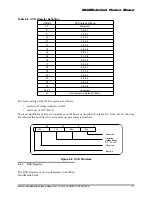
Страница 27: ...3 5 23 3 5 3 6 24 30 reserved 31 Card power up status bit busy The level coding of the OCR register is as follows restricted voltage windows LOW card busy LOW bit 31 The least significant 31 bits are constant and will be set as described in Figure 4 6 If set bit 32 the busy bit informs the host that the card power up procedure is finished 00h 24 00h 0 80h 8 FFh 16 Reserved Operating Voltage Range ...

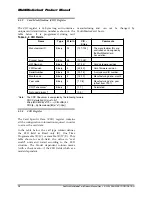
Страница 28: ...evision Serial Number Binary 24 39 16 A unique card ID number Month code Binary 4 15 12 Manufacturing date month Year code Binary 4 11 8 Manufacturing date year offset from 1997 CRC7 checksum Binary 7 7 1 Calculated Not used always 1 1 0 0 Note The CRC Checksum is computed by the following formula CRC Calculation G x x7 3 1 M x MID MSB x119 CIN LSB x0 CRC 6 0 Remainder M x x7 G x 4 5 4 CSD Registe...

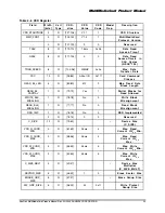
Страница 29: ...AD_BL_LEN 4 R 83 80 512 9 Max Read Data Block Length READ_BL_ PARTIAL 1 R 79 79 Yes 1 Partial Blocks for Read Allowed WRITE_BLK_ MISALIGN 1 R 78 78 No 0 Write Block Misalignment READ_BLK_ MISALIGN 1 R 77 77 No 0 Read Block Misalignment DSR_IMP 1 R 76 76 No 0 DSR Implemented 2 R 75 74 0 0 Reserved C_SIZE 12 R 73 62 Device Size C_SIZE VDD_R_CURR_ MIN 3 R 61 59 25ma 4 Max Read Current VDD Min VDD_R_C...

Страница 30: ...11 10 0 0 Reserved ECC 2 R W E 9 8 None 0 ECC Code CRC 7 R W E 7 1 CRC 1 0 0 1 1 Not Used Always 1 The following sections describe the CSD fields and the relevant data types If not explicitly defined otherwise all bit strings are interpreted as binary coded numbers starting with the left bit first CSD_STRUCTURE describes the version of the CSD structure Table 4 7 CSD Register Structure CSD_STRUCTU...

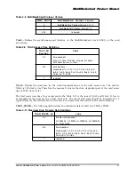
Страница 31: ...st case for the clock dependent factor of the data access time The unit for NSAC is 100 clock cycles Therefore the maximal value for the clock dependent part of the read access time is 25 5k clock cycles The total read access time NAC as expressed in the Table 5 12 is the sum of TAAC and NSAC It has to be computed by the host for the actual clock rate The read access time should be interpreted as ...

Страница 32: ...s that only the READ_BL_LEN block size can be used for block oriented data transfers READ_BL_PARTIAL 1 means that smaller blocks can be used as well The minimum block size will be equal to minimum addressable unit one byte WRITE_BLK_MISALIGN Defines if the data block to be written by one command can be spread over more than one physical block of the memory device The size of the memory block is de...

Страница 33: ..._R_CURR_MIN VDD_W_CURR_MIN The minimum values for read and write currents on VDD power supply are coded as follows Table 4 14 VDD Minimum Current Consumption VDD_R_CURR_MIN VDD_W_CURR_MIN Code For Current Consumption VD D 2 0 0 0 5mA 1 1mA 2 5mA 3 10mA 4 25mA 5 35mA 6 60mA 7 100mA VDD_R_CURR_MAX VDD_W_CURR_MAX The maximum values for read and write currents on VDD power supply are coded as follows ...

Страница 34: ...escribed later R2W_FACTOR Defines the typical block program time as a multiple of the read access time The following table defines the field format Table 4 17 R2W_FACTOR R2W_FACTOR Multiples of Read Access Time 0 1 1 2 write half as fast as read 2 4 3 8 4 16 5 32 6 7 reserved WRITE_BL_LEN Block length for write operations See READ_BL_LEN for field coding WRITE_BL_PARTIAL Defines whether partial bl...

Страница 35: ...hecksum has to be recalculated by the host for any CSD modification The default corresponds to the initial CSD contents 4 5 5 Status Register The MultiMediaCard status register structure is defined in the following table The Type and Clear Condition fields in the table are coded as follows Type E Error bit S Status bit R Detected and set for the actual command response X Detected and set during co...

Страница 36: ... 8 E X 0 no error 1 error The card could not sustain data transfer in stream read mode C 1 7 E X 0 no error 1 error The card could not sustain data programming in stream write mode C 1 6 E R 0 no error 1 error Can be one of the following errors The CID register has been already written and can not be overwritten The read only section of the CSD does not match the card content An attempt to reverse...

Страница 37: ...d by State with CMD7 4 5 7 MultiMediaCard Registers in SPI Mode In SPI mode only the MultiMediaCard CSD and CID registers are accessible Their format is identical to the format in the MultiMediaCard mode However a few fields are irrelevant in SPI mode In SPI mode the card status register has a different shorter format as well Refer to the SPI Protocol section for more details Table 4 20 MultiMedia...

Страница 38: ...conditions and timings are presented in the following sections Three operation modes are defined for MultiMediaCards Card Identification Mode The host will be in card identification mode after reset and while it is looking for new cards on the bus MultiMediaCards will be in this mode after reset until the SET_RCA command CMD3 is received Interrupt Mode The Interrupt Mode option defined in the Mult...

Страница 39: ...ommand and sets all MultiMediaCards to Idle State regardless of the current card state MultiMediaCards in Inactive State are not affected by this command After power on by the host all MultiMediaCards are in Idle State including the cards that were in Inactive State Note that at least 74 clock cycles are required prior to starting bus communication After power on or CMD0 all MultiMediaCards output...

Страница 40: ...s case the host must repeat CMD1 until the busy bit is cleared During the initialization procedure the host is not allowed to change the OCR values Changes in the OCR content will be ignored by the MultiMediaCard If there is a real change in the operating conditions the host must reset the card stack using CMD0 and begin the initialization procedure once more GO_INACTIVE_STATE CMD15 can also be us...

Страница 41: ... Figure 5 2 MultiMediaCard State Diagram Data Transfer Mode CMD7 is used to select one MultiMediaCard and place it in the Transfer State Only one MultiMediaCard can be in the Transfer State at a given time If a previously selected MultiMediaCard is in the Transfer State its connection with the host is released and it will move back to the Stand by State When CMD7 is issued with the reserved relati...

Страница 42: ...ull and as long as the MultiMediaCard is in Programming State see MultiMediaCard state diagram Figure 5 2 the DAT line will be kept low There is no buffering option for write CSD write CID write protection and erase This means that while the MultiMediaCard is busy servicing any one of these commands no other data transfer commands will be accepted DAT line will be kept low as long as the MultiMedi...

Страница 43: ...us register abort transmission and wait in the Data State for a stop command 1 All upper case names are defined in the CSD 5 3 2 Data Write Format The data transfer format is similar to the data read format For block oriented write data transfer the CRC check bits are added to each data block The card performs a CRC check for each such received data block prior to a write operation The polynomial ...

Страница 44: ...the unit of measure for determining an erase is either a sector or an erase group but if a sector all selected sectors must lie within the same erase group To facilitate selection a first command with the starting address is followed by a second command with the final address and a l l sectors within this range will be selected for erase After a range is selected an individual sector or group with...

Страница 45: ...command end bit A command with response 8 clocks after the card response end bit A read data transaction 8 clocks after the end bit of the last data block A write data transaction 8 clocks after the CRC status token The host is allowed to shut down the clock of a busy card The MultiMediaCard will complete the programming operation regardless of the host clock However the host must provide a clock ...

Страница 46: ...rst bit xn second bit xn 1 last bit x0 CRC 15 0 Remainder M x x16 G x All CRC registers are initialized to zero The first bit is the first data bit of the corresponding block The degree n of the polynomial denotes the number of bits of the data block decreased by one For example n 4 095 for a block length of 512 bytes The generator polynomial G x is a standard CCITT poly nomial The code has a mini...

Страница 47: ...host does not get a response within the defined time out it should assume the card is not going to respond any more and try to recover e g reset the card power cycle reject etc The typical access and program times are defined as follows Read The read access time is defined as the sum of the two times given by the CSD parameters TAAC and NSAC These card parameters define the typical delay between t...

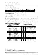
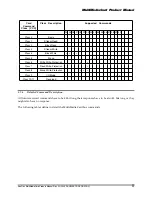
Страница 48: ...ses See Table 5 2 Each class supports a set of MultiMediaCard functions The supported Card Command Classes CCC are coded as a parameter in the card specific data CSD register of each card providing the host with information on how to access the card Table 5 2 Card Command Classes CCCs Card Command Class CCC Class Description Supported Commands 0 1 2 3 4 7 9 10 11 12 13 15 16 17 18 20 Class 0 Basic...

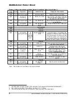
Страница 49: ...d Class 2 Block Read Class 3 Stream Write Class 4 Block Write Class 5 Erase Class 6 Write Write Protection Class 7 Read Write Protection Class 8 Erase Write Protection Class 9 I O Mode Class 10 11 Reserved 5 7 4 Detailed Command Description All future reserved commands have to be 48 bit long their responses have to be also 48 bits long or they might also have no response The following tables defin...

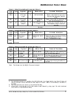
Страница 50: ...ases the card is selected by its own relative address and deselected by any other address address 0 deselects all CMD8 Reserved CMD9 ac 31 16 RCA 15 0 don t cares R2 SEND_CSD Addressed card sends its card specific data CSD on the CMD line CMD10 ac 31 16 RCA 15 0 don t cares R2 SEND_CID Addressed card sends its card identification CID on the CMD line CMD11 adtc 31 0 data address2 R1 READ_DAT_UNTIL_...

Страница 51: ...dress until a STOP_TRANSMISSION follows CMD21 CMD23 Reserved Table 5 6 Block Oriented Write Commands Class 4 Cmd Index Type Argument Resp Abbreviation Command Description CMD24 adtc 31 0 data address R1 WRITE_BLOCK Writes a block of the size selected by the SET_BLOCKLEN command 3 CMD25 adtc 31 0 data address R1 WRITE_MULTIPLE_ BLOCK Continuously writes blocks of data until a STOP_TRANSMISSION foll...

Страница 52: ...s of the last sector in a continuous range within the selected erase group or the address of a single sector to be selected for erase CMD34 ac 31 0 data address R1 UNTAG_SECTOR Removes one previously selected sector from the erase selection CMD35 ac 31 0 data address R1 TAG_ERASE_GROUP_ START Sets the address of the first erase group within a range to be selected for erase CMD36 ac 31 0 data addre...

Страница 53: ...stby class 0 CMD0 idle idle idle idle idle idle idle idle idle stby CMD1 card VDD range compatible ready stby CMD1 card is busy idle stby CMD1 card VDD range not compatible ina stby CMD2 card wins bus ident stby CMD2 card loses bus ready stby CMD3 stby stby CMD4 stby stby CMD7 card is addressed tran prg stby CMD7 card is not addressed stby stby dis stby CMD9 stby stby CMD10 stby stby CMD12 tran pr...

Страница 54: ... 11 CMD41 CMD59 Reserved CMD60 CMD63 Reserved for manufacturer 5 9 Responses All responses are sent via the CMD line The response transmission always starts with the MSB The response length depends on the response type A response always starts with a start bit always 0 followed by the bit indicating the direction of transmission card 0 A value denoted by x in the tables below indicates a variable ...

Страница 55: ... content of the CID register is sent as a response to CMD2 and CMD10 The content of the CSD register is sent as a response to CMD9 Only bits 127 1 of the CID and CSD are transferred bit 0 of these registers is replaced by the end bit of the response Bit Position 135 134 133 128 127 1 0 Width bits 1 1 6 127 1 Value 0 0 111111 x 1 Description start bit transmission bit reserved CID or CSD register i...

Страница 56: ...pectively RDAT Actively driven P bits are less sensitive to noise superposition All timing values are defined in Table 5 12 5 10 1 Command and Response Both host command and card response are clocked out with the rising edge of the host clock The minimum delay between the host command and card response is NCR clock cycles This timing diagram is relevant for host command CMD3 Host Command NCR Cycle...

Страница 57: ...CMD Start Data Transfer Mode Last Host Command Next Host Command Timing Diagram After the last command has been sent the host can continue sending the next command after at least NCC clock periods This timing is relevant for any host command that does not have a response Host Command NCC Cycles Host Command CMD S T Content CRC E Z Z S T Content CRC E Figure 5 9 Timing CMDn End to CMDn 1 Start All ...

Страница 58: ...ycles after the end bit of the host command The bus transaction is identical to that of a read block command see Figure 5 10 As the data transfer is not block oriented the data stream does not include the CRC checksum Consequently the host can not check for data validity The data stream is terminated by a stop command The corresponding bus transaction is identical to the stop command for the multi...

Страница 59: ... without card busy signal Figure 5 14 Timing of Multiple Block Write Command In write mode the stop transmission command works similarly to the stop transmission command in the read mode Figures 5 15 to 5 18 describe the timing of the stop command in different card states Figure 5 15 Stop Transmission During Data Transfer from the Host The card will treat a data block as successfully received and ...

Страница 60: ...received The bus transaction is identical to that of a write block command see Figure 5 13 As the data transfer is not block oriented the data stream does not include the CRC checksum Consequently the host can not receive any CRC status information from the card The data stream is terminated by a stop command The bus transaction is identical to the write block option when a data block is interrupt...

Страница 61: ...MediaCard mode is 1 The default block length is as specified in the CSD 512 bytes A set block length of less than 512 bytes will cause a write error The only valid write set block length is 512 bytes CMD16 is not mandatory if the default is accepted required it will not respond to the command and remain in the MultiMediaCard mode If SPI mode is required the card will switch to SPI mode and respond...

Страница 62: ...MultiMediaCard CMD17 Upon reception of a valid read command the card will respond with a response token followed by a data token in the length defined in a previous SET_BLOCK_LENGTH CMD16 command refer to Figure 6 1 From Host to Card From Card to Host Data From Card to Host Next Command DataIn DataOut Command Response Command Data Block CRC Figure 6 1 Read Operation A valid data block is suffixed ...

Страница 63: ...ion is completed the host must check the results of the programming using the SEND_STATUS command CMD13 Some errors e g address out of range write protect violation etc are detected during programming only The only validation check performed on the data block and communicated to the host via the data response token is CRC Resetting the CS signal while the card is busy will not terminate the progra...

Страница 64: ...last SPI bus transaction the host is required to provide 8 eight clock cycles for the card to complete the operation before shutting down the clock Throughout this 8 clock period the state of the CS signal is irrelevant It can be asserted or deasserted Following is a list of the various SPI bus transactions A command response sequence Eight clocks after the card response end bit The CS signal can ...

Страница 65: ...ut and the maximum frequency for stream read Write The R2W_FACTOR field in the CSD is used to calculate the typical block program time obtained by multiplying the read access time by this factor It applies to all write erase commands e g SET CLEAR _WRITE_PROTECT PROGRAM_CSD CID and the block write commands It should be used by the host to calculate throughput and the maximum frequency for stream w...

Страница 66: ... None R1 GO_IDLE_STATE Resets the MultiMediaCard CMD1 Yes None R1 SEND_OP_COND Activates the card s initialization process CMD2 No CMD3 No CMD4 No CMD5 reserved CMD6 reserved CMD7 No CMD8 reserved CMD9 Yes None R1 SEND_CSD Asks the selected card to send its card specific data CSD CMD10 Yes None R1 SEND_CID Asks the selected card to send its card identification CID CMD11 No CMD12 No CMD13 Yes None ...

Страница 67: ... 5 CMD31 reserved CMD32 Yes 31 0 data address R1 TAG_SECTOR_ START Sets the address of the first sector of the erase group CMD33 Yes 31 0 data address R1 TAG_SECTOR_ END Sets the address of the last sector in a continuous range within the selected erase group or the address of a single sector to be selected for erase CMD34 Yes 31 0 data address R1 UNTAG_SECTOR Removes one previously selected secto...

Страница 68: ...of the R1 format is given in Figure 6 5 In idle state The card is in idle state and running initializing process Erase reset An erase sequence was cleared before executing because an out of erase sequence command was received Illegal command An illegal command code was detected Communication CRC error The CRC check of the last command failed Erase sequence error An error in the sequence of erase c...

Страница 69: ...response R1 The content of the second byte is described below Erase param An invalid selection sectors or groups for erase Write protect violation The command tried to write a write protected block Card ECC failed Card internal ECC was applied but failed to correct the data CC error Internal card controller error Error A general or an unknown error occurred during the operation Write protect erase...

Страница 70: ...the data block length User data Last two bytes 16 bit CRC 6 2 4 Data Error Token If a read operation fails and the card cannot provide the required data it will sent a data error token instead This token is one byte long and has the following format Error CC_Error Card_ECC_Failed Out_of_Range 7 0 0 0 0 0 Figure 6 7 Data Error Token The 4 LSBs are the same error bits as in response format R2 6 3 Ca...

Страница 71: ...0 X Don t care Z high impedance state 1 repeater Busy Busy Token Command Command token Response Response token Data block Data token All timing values are defined in Table 6 2 The host must keep the clock running for at least NCR clock cycles after the card response is received This restrictions applied to command and data response tokens 6 4 1 Command Response Host Command to Card Response Card i...

Страница 72: ...72 Card Response to Host Command 6 4 2 Data Read 6 4 2 1 Data Write 6 4 3 Timing Values Table 6 2 Timing Constants Definitions Min Max Unit NCS 0 8 clock cycles NCR 1 8 8 clock cycles NRC 1 8 clock cycles NAC 1 10 TAAC NSAC 8 clock cycles NWR 1 8 clock cycles NEC 0 8 clock cycles NDS 0 8 clock cycles ...

Страница 73: ...TION 73 6 5 SPI Electrical Interface The SPI Mode electrical interface is identical to that of the MultiMediaCard mode 6 6 SPI Bus Operating Conditions Identical to MultiMediaCard mode 6 7 Bus Timing Identical to MultiMediaCard mode The timing of the CS signal is the same as any other card input ...

Страница 74: ...MultiMediaCard Product Manual SanDisk MultiMediaCard Product Manual Rev 2 2000 SANDISK CORPORATION 74 ...

Страница 75: ...SanDisk MultiMediaCard Product Manual Rev 2 2000 SANDISK CORPORATION 75 Ordering Information and Technical Support ...

Страница 76: ...76 SanDisk MultiMediaCard Product Manual Rev 2 2000 SANDISK CORPORATION ...

Страница 77: ...rt SanDisk MultiMediaCard Product Manual Rev 2 2000 SANDISK CORPORATION 77 Ordering Information To order SanDisk products directly from SanDisk call 408 542 0595 MultiMediaCard Model SDMB 4 4 0 MB SDMB 8 8 0 MB SDMB 16 16 0 MB SDMB 32 32 1MB ...

Страница 78: ...5 for technical support SanDisk Worldwide Web Site Internet users can obtain technical support and product information along with SanDisk news and much more from the SanDisk Worldwide Web Site 24 hours a day seven days a week The SanDisk Worldwide Web Site is frequently updated Visit this site often to obtain the most up to date information on SanDisk products and applications The SanDisk Web Site...

Страница 79: ...SanDisk MultiMediaCard Product Manual Rev 2 2000 SANDISK CORPORATION 79 SanDisk Sales Offices ...

Страница 80: ...SanDisk Worldwide Sales Offices SanDisk MultiMediaCard Product Manual Rev 2 2000 SANDISK CORPORATION 80 ...

Страница 81: ...Latin South America 407 667 4880 FAX 407 667 4834 Europe SanDisk GmbH Karlsruher Str 2C D 30519 Hannover Germany 49 511 8759185 FAX 49 511 8759187 SanDisk Northern Europe Videroegaten 3 B S 16440 Kista Sweden 46 0 8 75084 63 FAX 46 0 8 75084 26 SanDisk Central Europe Eutelis Plaz 3 D 40878 Ratingen Germany 49 2102 999666 FAX 49 2102 999667 Japan SanDisk K K 8F Nisso Bldg 15 2 17 19 Shin Yokohama K...

Страница 82: ...SanDisk Worldwide Sales Offices SanDisk MultiMediaCard Product Manual Rev 2 2000 SANDISK CORPORATION 82 ...

Страница 83: ... defective within one year of purchase SanDisk will have the option of repairing or replacing the defective product if the following conditions are met A A warranty registration card for each defective product was submitted and is on file at SanDisk If not a warranty registration card must accompany each returned defective product This card is included in each product s original retail package B T...

Страница 84: ...oved SanDisk will issue a Return Material Authorization or Product Repair Authorization number Ship the defective product to SanDisk Corporation Attn RMA Returns Reference RMA or PRA 140 Caspian Court Sunnyvale CA 94089 V STATE LAW RIGHTS SOME STATES DO NOT ALLOW THE EXCLUSION OR LIMITATION OF INCIDENTAL OR CONSEQUENTIAL DAMAGES OR LIMITATION ON HOW LONG AN IMPLIED WARRANTY LASTS SO THE ABOVE LIMI...

Страница 85: ...s MultiMediaCard Connector Vendors Company Contact Phone Fax ITT Cannon Greg Maslak 612 974 5833 612 934 9121 Yamaichi Electronics Derrick Simpson 408 456 0797 408 456 0799 AVX Kyocera ELCO Connectors Tom Anderson 843 946 0351 843 626 5814 AMP TYCO Kirk D Ulery 717 592 6736 717 592 5266 JST Corporation Steve Gazay 408 734 7902 408 734 7901 ...

Страница 86: ...Appendix MultiMediaCard Connectors SanDisk MultiMediaCard Product Manual Rev 2 2000 SANDISK CORPORATION 86 MultiMediaCard Host Connector ...

Отзывы: