3-3
Samsung Electronics
CIRCUIT DESCRIPTION
Repair Manual
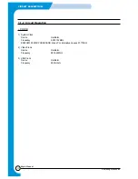
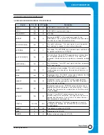
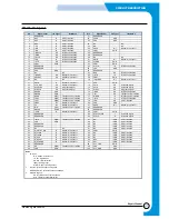
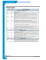
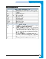
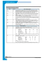
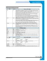
• KS32C65100 MICROPROCESSOR
1) KS32C65100 MICROPROCESSOR PIN & INTERFACE
Signal
Pin No.
I/O Type
Description
OSCI
184
I7
KS32C65100 master clock input.
OSCO
185
O7
KS32C65100 master clock output.
PLL_FILTER
183
I5
PLL filter
nRESET
182
I4
Not reset. nRESET is the global reset input for the
KS32C65100. For a system reset, nRESET must be held to
low level for at least 65 machine cycles.
nSLCTIN/GIP[16]
152
I1
Not select information. This input signal is used by parallel
port interface to request 'on-line' status information.
nSTROBE
151
I1
Not strobe. The nSTROBE input indicates when valid data is
on parallel port data bus, PPD[7:0]
nAUTOFD/GIP[17]
154
I1
Not auto feed. The nAUTOFD input indicates whether data
on the parallel port data bus, PPD[7:0], is an auto feed
command. Otherwise, the bus signals are interpreted as data
only.
nINIT/GIP[15]
153
I1
Not initialization. The nINIT input signal initializes the parallel
port's input control.
nACK
159
I1
Not parallel port acknowledge. The nACK output signal is
issued whenever a transfer on the parallel port data bus is
completed.
BUSY
158
O1
Parallel port busy. The BUSY output signal indicates that the
KS32C65100 parallel port is currently busy.
SELECT
156
O1
Parallel port select. The SELECT output signal indicates
whether the device connected to the KS32C65100 parallel
port is 'on-line' or 'off-line'.
PERROR
157
O1
Parallel port paper error. PERROR output indicates that a
problem exists with the paper in the ink-jet printer. It could
indicate that the printer has a paper jam or that the printer
is out of paper.
nFAULT
155
O1
Not fault. The nFAULT output indicates that an error
condition exists with the printer. This signal can be used to
indicate that the printer is out of ink or to inform the user
that the printer is not turned on.
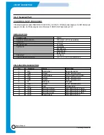
PPD[7:0]
142~149
I/O2
arallel port data bus. This 8-bit, tri-state bus is used to
exchange data between the KS32C65100 and an external
host(peripheral).
SAVRT
2
I6
Top reference voltage for IP ADC
SAIN
3
I6
Analog input for IP ADC
SAVRB
4
I6
Bottom reference voltage for IP ADC
Содержание SF-530 Series
Страница 87: ...Electronics ...
Страница 128: ...4 2 SCHEMATIC DIAGRAMS Samsung Electronics Repair Manual 4 2 Main Circuit Diagram 2 6 APOLLO2 MAIN ...
Страница 129: ...4 3 Samsung Electronics SCHEMATIC DIAGRAMS Repair Manual 4 3 Main Circuit Diagram 3 6 APOLLO2 MAIN ...
Страница 130: ...4 4 SCHEMATIC DIAGRAMS Samsung Electronics Repair Manual 4 4 Main Circuit Diagram 4 6 APOLLO2 MAIN ...
Страница 131: ...4 5 Samsung Electronics SCHEMATIC DIAGRAMS Repair Manual 4 5 Main Circuit Diagram 5 6 APOLLO2 MAIN ...
Страница 132: ...4 6 SCHEMATIC DIAGRAMS Samsung Electronics Repair Manual 4 6 Main Circuit Diagram 6 6 APOLLO2 MAIN ...
Страница 133: ...4 7 Samsung Electronics SCHEMATIC DIAGRAMS Repair Manual 4 7 LIU Circuit Diagram 1 2 APOLLO2 LIU ...
Страница 134: ...4 8 SCHEMATIC DIAGRAMS Samsung Electronics Repair Manual 4 8 LIU Circuit Diagram 2 2 APOLLO2 LIU ...
Страница 136: ...4 10 SCHEMATIC DIAGRAMS Samsung Electronics Repair Manual 4 10 Scan Circuit Diagram 200DPI APOLLO2 200DPI ...
Страница 137: ...4 11 Samsung Electronics SCHEMATIC DIAGRAMS Repair Manual 4 11 Scan Circuit Diagram 300DPI APOLLO2 300DPI ...

