1-3 Precautions for Electrostatically Sensitive Devices (ESDs)
1. Some semiconductor (“solid state”) devices
are easily damaged by static electricity. Such
components are called Electrostatically
Sensitive Devices (ESDs); examples include
integrated circuits and some field-effect
transistors. The following techniques will
reduce the occurrence of component damage
caused by static electricity.
2. Immediately before handling any semicon
ductor components or assemblies, drain the
electrostatic charge from your body by
touching a known earth ground. Alternatively,
wear a discharging wrist-strap device. (Be
sure to remove it prior to applying power—
this is an electric shock precaution.)
3. After removing an ESD-equipped assembly,
place it on a conductive surface such as
aluminum foil to prevent accumulation of
electrostatic charge.
4. Do not use freon-propelled chemicals. These
can generate electrical charges that damage
ESDs.
5. Use only a grounded-tip soldering iron when
soldering or unsoldering ESDs.
6. Use only an anti-static solder removal device.
Many solder removal devices are not rated as
“anti-static”; these can accumulate sufficient
electrical charge to damage ESDs.
7. Do not remove a replacement ESD from its
protective package until you are ready to
install it. Most replacement ESDs are
packaged with leads that are electrically
shorted together by conductive foam,
aluminum foil or other conductive materials.
8. Immediately before removing the protective
material from the leads of a replacement ESD,
touch the protective material to the chassis or
circuit assembly into which the device will be
installed.
9. Minimize body motions when handling
unpackaged replacement ESDs. Motions such
as brushing clothes together, or lifting a foot
from a carpeted floor can generate enough
static electricity to damage an ESD.
Precautions
1-4
Samsung Electronics
Содержание PCJ522R
Страница 2: ...ELECTRONICS Samsung Electronics Co Ltd JUL 2000 Printed in Korea 3P51A 6510 ...
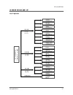
Страница 28: ...Alignment and Adjustments Samsung Electronics 4 13 4 5 Screen Jig 4 5 1 43J5P 4 5 2 43J5P DTV Mode ...
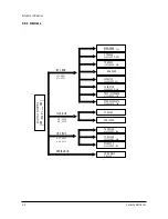
Страница 29: ...Alignment and Adjustments 4 14 Samsung Electronics 4 5 3 53J5P 4 5 4 53J5P DTV Mode ...
Страница 30: ...Alignment and Adjustments Samsung Electronics 4 15 4 5 5 61J5P 4 5 6 61J5P DTV ...
Страница 31: ...Alignment and Adjustments 4 16 Samsung Electronics 4 5 7 552W 4 5 8 552W DTV Mode ...
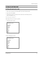
Страница 32: ...Alignment and Adjustments Samsung Electronics 4 17 4 6 Remote Control for Servicing Convergence Mode ...
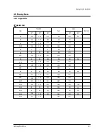
Страница 35: ...Alignment and Adjustments 4 20 Samsung Electronics 4 7 Convergence Adjustment ...
Страница 36: ...Alignment and Adjustments Samsung Electronics 4 21 ...
Страница 37: ...Alignment and Adjustments 4 22 Samsung Electronics ...
Страница 38: ...Alignment and Adjustments Samsung Electronics 4 23 ...
Страница 39: ...Alignment and Adjustments 4 24 Samsung Electronics ...
Страница 40: ...Alignment and Adjustments Samsung Electronics 4 25 ...
Страница 41: ...Alignment and Adjustments 4 26 Samsung Electronics 4 8 PC Mode 4 8 1 TV Setup Mode ...
Страница 57: ...Alignment and Adjustments 4 42 Samsung Electronics 4 9 9 3D PHONIC Module 4 9 10 MTS Module ...
Страница 63: ...MEMO 5 4 Samsung Electronics ...
Страница 112: ...8 4 Samsung Electronics MEMO ...
Страница 116: ...Schematic Diagrams Samsung Electronics 10 3 10 3 MAIN C TP03 TP02 TP01 TP04 Power Line Signal Line TP01 TP02 TP03 TP04 ...
Страница 117: ...Schematic Diagrams 10 4 Samsung Electronics 10 4 MAIN D TP01 TP03 TP02 Power Line Signal Line TP01 TP02 TP03 ...
Страница 119: ...Schematic Diagrams 10 6 Samsung Electronics 10 6 SUB POWER DEFL 2 TP01 Power Line Signal Line TP01 ...
Страница 120: ...Schematic Diagrams Samsung Electronics 10 7 10 7 CRT ...
Страница 122: ...Schematic Diagrams Samsung Electronics 10 9 10 9 CONVERGENCE MDL ...
Страница 123: ...Schematic Diagrams 10 10 Samsung Electronics 10 10 HV MODULE TP01 TP02 Power Line Signal Line TP01 TP02 ...
Страница 124: ...Schematic Diagrams Samsung Electronics 10 11 10 11 3D COMB 7 7 Power Line Signal Line ...
Страница 125: ...Schematic Diagrams 10 12 Samsung Electronics 10 12 3D PHONIC ...
Страница 126: ...Schematic Diagrams Samsung Electronics 10 13 10 13 F CONVERTER ...
Страница 127: ...Schematic Diagrams 10 14 Samsung Electronics 10 14 PIP ...
Страница 128: ...Schematic Diagrams Samsung Electronics 10 15 10 15 TERMINAL 1 ...
Страница 129: ...Schematic Diagrams 10 16 Samsung Electronics 10 16 TERMINAL 2 ...
Страница 130: ...Schematic Diagrams Samsung Electronics 10 17 10 17 IF V M MODULE ...
Страница 131: ...Schematic Diagrams 10 18 Samsung Electronics 10 18 PROSCAN 1 3 ...
Страница 132: ...Schematic Diagrams Samsung Electronics 10 19 10 19 PROSCAN 2 3 Power Line Signal Line ...
Страница 133: ...Schematic Diagrams 10 20 Samsung Electronics 10 20 PROSCAN 3 3 Power Line Signal Line ...
Страница 134: ...Schematic Diagrams Samsung Electronics 10 21 10 21 CHROMA INTERLACE ONLY ...

