Alignment and Adjustments
4-10
Samsung Electronics
4-4 Other Adjustments
4-4-1 Screen Adjustment
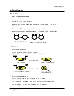
1. Warm up the TV for at least 30 minutes.
2. Turn to the Video Mode (No Signal) using a
remote-control.
3. Connect an oscilloscope to RK,GK,BK.
4. Adjust the VR (VR501, VR531, VR561) screen
so that RK, GK, BK pulse is 20Vp-p each.
(Turn the R,G,B VR screen fully
counterclockwise in the area of each flyback
line.)
4-4-2 White Balance Adjustment
1. Select the “STANDARD” video mode.
2. Input 100% white pattern.
3. In the stand-by mode, press the remote-control
keys in the following sequence:
Mute
→
1
→
8
→
2
→
Power ON
4. Warm up the TV for at least 30 minutes.
5. Input a 10-step signal.
6. R-cut off, B-cut off, and G-cut off by pressing
the /- keys.
7. Adjust the low light with viewing the dark
side of the screen.
8. Select R-drive, G-drive, and B-drive by
pressing the /- keys.
9. Adjust the high light with viewing the light
side of the screen.
10. If necessary, redo adjustments 6~9.
11. Press the Menu key to exit.
4-4-3 Sub-Brightness Adjustment
1. Input a sub-brightness adjustment signal.
(TOSHIBA PATTERN)
2. In the stand-by mode, press the remote-control
keys in the following sequence :
Mute - 1 - 8 - 2 - Power ON
3. Select SBT by pressing the /- keys.
4. Adjust so that the 7th step on the right side of
the screen is not seen (Use the /-
keys).
5. Press the Menu key to exit.
4-4-4 High Voltage (31KV) Check
PRECAUTION
1. Input a lion head pattern.
2. Select “STANDARD” video mode.
3. Warm up the TV for at least 10 minutes.
4. Use a 1000:1 probe.
ADJUSTMENT
1. Connect the (+) terminal of the 1000:1 probe to
the high voltage distributor and the (-)
terminal to GND (located on the deflection
board).
2. Adjust VR471 (located on the deflection board)
so that the digital meter indicates
DC 31V
±
0.1V.
Содержание PCJ522R
Страница 2: ...ELECTRONICS Samsung Electronics Co Ltd JUL 2000 Printed in Korea 3P51A 6510 ...
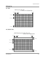
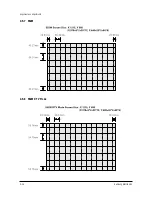
Страница 28: ...Alignment and Adjustments Samsung Electronics 4 13 4 5 Screen Jig 4 5 1 43J5P 4 5 2 43J5P DTV Mode ...
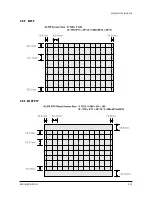
Страница 29: ...Alignment and Adjustments 4 14 Samsung Electronics 4 5 3 53J5P 4 5 4 53J5P DTV Mode ...
Страница 30: ...Alignment and Adjustments Samsung Electronics 4 15 4 5 5 61J5P 4 5 6 61J5P DTV ...
Страница 31: ...Alignment and Adjustments 4 16 Samsung Electronics 4 5 7 552W 4 5 8 552W DTV Mode ...
Страница 32: ...Alignment and Adjustments Samsung Electronics 4 17 4 6 Remote Control for Servicing Convergence Mode ...
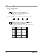
Страница 35: ...Alignment and Adjustments 4 20 Samsung Electronics 4 7 Convergence Adjustment ...
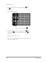
Страница 36: ...Alignment and Adjustments Samsung Electronics 4 21 ...
Страница 37: ...Alignment and Adjustments 4 22 Samsung Electronics ...
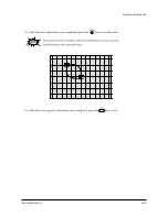
Страница 38: ...Alignment and Adjustments Samsung Electronics 4 23 ...
Страница 39: ...Alignment and Adjustments 4 24 Samsung Electronics ...
Страница 40: ...Alignment and Adjustments Samsung Electronics 4 25 ...
Страница 41: ...Alignment and Adjustments 4 26 Samsung Electronics 4 8 PC Mode 4 8 1 TV Setup Mode ...
Страница 57: ...Alignment and Adjustments 4 42 Samsung Electronics 4 9 9 3D PHONIC Module 4 9 10 MTS Module ...
Страница 63: ...MEMO 5 4 Samsung Electronics ...
Страница 112: ...8 4 Samsung Electronics MEMO ...
Страница 116: ...Schematic Diagrams Samsung Electronics 10 3 10 3 MAIN C TP03 TP02 TP01 TP04 Power Line Signal Line TP01 TP02 TP03 TP04 ...
Страница 117: ...Schematic Diagrams 10 4 Samsung Electronics 10 4 MAIN D TP01 TP03 TP02 Power Line Signal Line TP01 TP02 TP03 ...
Страница 119: ...Schematic Diagrams 10 6 Samsung Electronics 10 6 SUB POWER DEFL 2 TP01 Power Line Signal Line TP01 ...
Страница 120: ...Schematic Diagrams Samsung Electronics 10 7 10 7 CRT ...
Страница 122: ...Schematic Diagrams Samsung Electronics 10 9 10 9 CONVERGENCE MDL ...
Страница 123: ...Schematic Diagrams 10 10 Samsung Electronics 10 10 HV MODULE TP01 TP02 Power Line Signal Line TP01 TP02 ...
Страница 124: ...Schematic Diagrams Samsung Electronics 10 11 10 11 3D COMB 7 7 Power Line Signal Line ...
Страница 125: ...Schematic Diagrams 10 12 Samsung Electronics 10 12 3D PHONIC ...
Страница 126: ...Schematic Diagrams Samsung Electronics 10 13 10 13 F CONVERTER ...
Страница 127: ...Schematic Diagrams 10 14 Samsung Electronics 10 14 PIP ...
Страница 128: ...Schematic Diagrams Samsung Electronics 10 15 10 15 TERMINAL 1 ...
Страница 129: ...Schematic Diagrams 10 16 Samsung Electronics 10 16 TERMINAL 2 ...
Страница 130: ...Schematic Diagrams Samsung Electronics 10 17 10 17 IF V M MODULE ...
Страница 131: ...Schematic Diagrams 10 18 Samsung Electronics 10 18 PROSCAN 1 3 ...
Страница 132: ...Schematic Diagrams Samsung Electronics 10 19 10 19 PROSCAN 2 3 Power Line Signal Line ...
Страница 133: ...Schematic Diagrams 10 20 Samsung Electronics 10 20 PROSCAN 3 3 Power Line Signal Line ...
Страница 134: ...Schematic Diagrams Samsung Electronics 10 21 10 21 CHROMA INTERLACE ONLY ...

