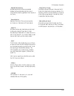
- TFT-LCD
(Thin film Transistor Liquid Crystal Display)
ADC(Analog to Digital Converter)
This is a circuit that converts from analog signal to
digital signals.
- PLL(Phase Locked Loop)
During progressing ADC, Device makes clock syn-
chronizing HSYNC with Video clock
- Inverter
Device that supply Power to LCD panel lamp. this
device gernerate about 1,500~2,000V.
- AC Adapter
Device that converts AC(90V~240V) to DC(+12V
or 14V)
- SMPS(Switching Mode Power Supply)
Switching Mode Power supply. This design tech-
nology is used to step up/down the input power by
switching on/off
- FRC(Frame Rate Controller)
Technology that change image frame quantity dis-
played on screen for one second.
Actually TFT-LCD panel require 60 pcs of frame
for one second.
so,this technology is needed to convert input
image to 60 pcs regardless input frame quantity.
- Image Scaler
Technology that convert various input resolution to
other resolution.(ex. 640* 480 to 1024*768)
- Auto Configuration(Auto adjustment)
This is an algorithm to adjust monitor to optimum
condition by pushing one key.
- OSD(On Screen Display)
On screen display. customer can control the
screen easily with this.
- Image Lock
This means "Fineness adjustment" in LCD
Monitor, the features are "Fine" and "Coarse"
- FINE
"Fine" adjustment is used to adjust visibility by
control phase difference.
- COARSE
This is a adjustment by tuning with Video colck
and PLL clock.
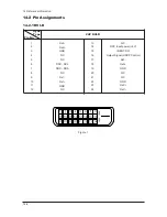
- DVI (Digital Visual Interface)
This provides a high speed digital connection for
visual data types that is display technology
independent. this interface is primarily forcused at
providing a connection between a computer and
its display device.
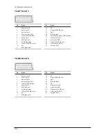
- L.V.D.S.(Low Voltage Differential Signaling)
a kind of transmission method for Digital.It can be
used from Main PBA to Panel.
- DVI (Digital Visual Interface)
This provides a high speed digital connection for
visual data types that is display technology inde-
pendent. this interface is primarily forcused at pro-
viding a connection between a computer and its
display device.
14 Reference Infomation
14-1
14 Reference Infomation
14-1 Technical Terms
Содержание LE23R87BD
Страница 35: ...11 Disassembly and Reassembly 11 4 Description Picture Description 6 Remove screws and lift up the BRKT ...
Страница 37: ...11 Disassembly and Reassembly 11 6 Memo ...
Страница 40: ...13 Circuit Descriptions 13 3 13 2 Main Block ...
Страница 47: ...13 Circuit Descriptions 13 10 13 3 9 HOT Balance Block Diagram 13 3 10 COLD Balance Block Diagram ...
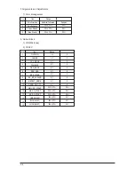
Страница 79: ...14 Reference Infomation 14 8 14 3 2 Supported Modes 1 ...
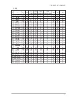
Страница 80: ...14 Reference Infomation 14 9 14 3 3 Supported Modes 2 ...
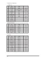
Страница 81: ...14 Reference Infomation 14 10 14 3 4 Supported Modes 3 ...
Страница 87: ...Memo 14 Reference Infomation 14 16 ...
Страница 88: ...7 Block Diagrams 7 1 7 Block Diagram This Document can not be used without Samsung s authorization ...
Страница 89: ...7 Block Diagrams 7 2 Memo ...
Страница 101: ...2 Product Specifications 2 12 Memo ...
Страница 104: ...5 Exploded View Parts List 5 3 5 3 LE26R86BD Exploded View T0003 T0175 M0215 T0447 M0115 M0014 M0107 M0013 M0013 ...
Страница 106: ...5 Exploded View Parts List 5 5 5 5 LE32R86BD Exploded View T0003 M0215 T0447 M0115 M0013 M0013 ...
Страница 108: ...5 Exploded View Parts List 5 7 5 7 LE37R87BD Exploded View T0003 M0215 M0013 M0013 T0447 M0115 M0146 M0146 M0107 M0014 ...
Страница 110: ...5 Exploded View Parts List 5 9 5 9 LE40R87BD Exploded View T0003 M0215 M0013 M0013 T0447 M0146 M0146 M0107 M0014 ...
Страница 112: ...12 PCB Diagram 12 1 12 PCB Diagram 12 1 Main PCB Diagram FOR READY ...
Страница 113: ...12 PCB Diagram 12 2 12 2 Main PCB Diagram FOR IDTV ...
Страница 114: ...12 PCB Diagram 12 3 12 3 23 SMPS ...
Страница 115: ...12 PCB Diagram 12 4 12 4 26 32 SMPS ...
Страница 116: ...12 PCB Diagram 12 5 12 5 37 SMPS ...
Страница 117: ...12 PCB Diagram 12 6 12 6 40 IP Board ...

