background image


RTD Embedded Technologies, Inc. 

www.rtd.com


7


ERES35105 

User’s Manual


1


Introduction


Product Overview 

The ERES35105 provides a direct interface to two Synchro/Resolver/LVDT channels on the compact PC/104 form factor with a stackable PCI 
Express bus. Both sensor input channels are independently configurable with jumpers. An onboard solid state Scott-T circuitry provides a 
precision conversion from Synchro to Resolver signals. Onboard precision thin-film resistor divider networks for 2.0, 11.8 or 90.0 V

RMS


configurations. 

The onboard programmable sine wave oscillator reference outputs a 0 - 7V

RMS

 excitation signal with a programmable frequency range of 0 Hz 

to 10 kHz. 


Board Features 


PC/104 form factor 


PCIe/104 stackable bus structure  

o


PCIe/104 Universal Connector 

o


Uses a PCIe x1 link 

o


Repopulates the PCIe bus 


2 Independent Channels 


Directly interfaces to Synchros, Resolvers and LVDTs 


Connection to 2.0V/11.8V/90.0V sensors 


Programmable resolution 10/12/14/16 - bits 


+5V only operation 


Programmable sine wave excitation  

o


0 Hz to 10 kHz frequency range 

o


0V to 7V

RMS

 voltage range 

o


Up to 100mA drive current at 85C 


Dual software selectable filters can be changed on-the-fly  

o


High Resolution mode for 16-bit resolution 

o


High Velocity mode for tracking rate up to 320 rps 

o


Other filter options available 


Synthesized reference corrects for phase shift up to 45 degrees 


Loss of signal detection 


Single-ended or Differential Inputs 


PCI Express (PCIe) x1 Upstream Interface to CPU  


Ordering Information 

The ERES35105 is available with the following options: 

Table 1: Ordering Options  

Part Number 

Description 

ERES35105HR-1 

PCIe/104 Two-Channel, 11.8 V

RMS

 Synchro/Resolver to Digital Peripheral Module 

ERES35105HR-2 

PCIe/104 Two-Channel, 90.0 V

RMS

 Synchro/Resolver to Digital Peripheral Module 

ERES35105HR-3 

PCIe/104 Two-Channel, 2.0  V

RMS

 Synchro/Resolver to Digital Peripheral Module 

IDAN- ERES35105HR-1S 

PCIe/104 Two-Channel, 11.8  V

RMS

 Synchro/Resolver to Digital Peripheral Module in IDAN enclosure 

IDAN- ERES35105HR-2S 

PCIe/104 Two-Channel, 90.0 V

RMS

 Synchro/Resolver to Digital Peripheral Module in IDAN enclosure 

IDAN- ERES35105HR-3S 

PCIe/104 Two-Channel, 2.0  V

RMS

 Synchro/Resolver to Digital Peripheral Module in IDAN enclosure 


The Intelligent Data Acquisition Node (IDAN™) building 

block can be used in just about any combination with other IDAN building blocks to 

create a 

simple but rugged 104™ stack.  This module can also be incorporated in a custom

-

built RTD HiDAN™ or HiDANplus

®

 High Reliability 

Intelligent Data Acquisition Node.  Contact RTD sales for more information on our high reliability systems. 

Содержание ERES35105HR

Страница 1: ...RTD Embedded Technologies Inc AS9100 and ISO 9001 Certified ERES35105HR PCI Express Dual Synchro Resolver LVDT Interface User s Manual BDM 610020152 Rev A...

Страница 2: ...RTD Embedded Technologies Inc 103 Innovation Boulevard State College PA 16803 USA Telephone 814 234 8087 Fax 814 234 5218 www rtd com sales rtd com techsupport rtd com...

Страница 3: ...emarks of PCI SIG PC 104 PC 104 Plus PCI 104 PCIe 104 PCI 104 Express and 104 are trademarks of the PC 104 Consortium All other trademarks appearing in this document are the property of their respecti...

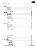
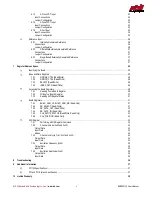
Страница 4: ...CN1 Top CN2 Bottom PCIe Connector 13 3 3 3 Jumpers 13 Steps for Installing 14 4 IDAN Connections 15 Module Handling Precautions 15 Physical Characteristics 15 Connector Locations 16 Connectors 16 4 4...

Страница 5: ...SELECT Read Write 28 7 2 4 INDEX_DATA Read Write 29 Accessing the Board Registers 29 7 3 1 Reading from a Board Register 29 7 3 2 Writing to a Board Register 30 7 3 3 Reading Shift Register Status 31...

Страница 6: ...esolver Jumper Settings 21 Table 10 Synchro Input Connections 22 Table 11 Synchro Jumper Settings 22 Table 12 2 Wire LVDT Input Connections 23 Table 13 2 Wire LVDT Jumper Settings 23 Table 14 3 Wire L...

Страница 7: ...de for 16 bit resolution o High Velocity mode for tracking rate up to 320 rps o Other filter options available Synthesized reference corrects for phase shift up to 45 degrees Loss of signal detection...

Страница 8: ...gh Friday 8 00am to 5 00pm EST E Mail sales rtd com 1 4 2 TECHNICAL SUPPORT If you are having problems with your system please try the steps in the Troubleshooting section of this manual on page 28 Fo...

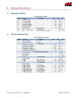
Страница 9: ...sumption Vcc5 5 0V 3 5 W Icc5 5V Input Supply Current Active 700 mA PCIe Bus Differential Output Voltage 0 8 1 2 V DC Differential TX Impedance 95 2 116 9 Differential Input Voltage 0 175 3 3 V DC Dif...

Страница 10: ...CI Express Port menu Contact your CPU vendor for details Board Handling Precautions To prevent damage due to Electrostatic Discharge ESD keep your board in its antistatic bag until you are ready to in...

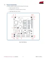
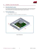
Страница 11: ...Physical Characteristics STEP model is available upon request contact RTD Tech Support for more information Weight Approximately 0 16 lbs 72 g Dimensions 90 17 mm L x 95 89 mm W 3 550 in L x 3 775 in...

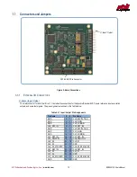
Страница 12: ...pin assignments are shown in the Table below Table 4 J1 Input Output Pin Assignments Pin Name Pin Name GND 2 1 CH0_EXCITATION GND 4 3 CH0_SINE GND 6 5 CH0_COSINE CH0_REF_IN 8 7 CH0_REF_IN GND 10 9 CH...

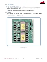
Страница 13: ...05 is a Universal board and can connect to either a Type 1 or Type 2 PCIe 104 connector 3 3 3 JUMPERS On all jumpers pin 1 is designated by a thick white silkscreen line and a square pad on the PCB Th...

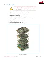
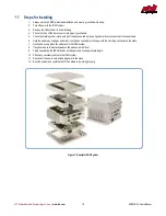
Страница 14: ...e on the stack 4 Remove the module from its anti static bag 5 Check that pins of the bus connector are properly positioned 6 Check the stacking order make sure all of the busses used by the peripheral...

Страница 15: ...nstall it into your system When removing it from the bag hold the module by the aluminum enclosure and do not touch the components or connectors Handle the module in an antistatic environment and use...

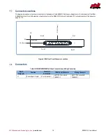
Страница 16: ...nnector on the ERES35105 refer to the External I O Connectors section of this manual on page 3 3 112 Figure 6 IDAN Front Panel Connector Locations Connectors Table 5 IDAN ERES35105HR xS Panel Connecto...

Страница 17: ...7 10 CH0_S1 19 11 GND 21 12 CH0_S2_RESOLVER 23 13 CH0_REF_IN 25 14 CH1_S1 27 15 GND 29 16 CH1_S2_RESOLVER 31 17 GND 33 18 RESERVED 19 RESERVED 20 GND 2 21 GND 4 22 GND 6 23 CH0_REF_IN 8 24 GND 10 25 G...

Страница 18: ...ripheral cards are connected to the cpuModule 6 Hold the module by its edges and orient it so the bus connector pins line up with the matching connector on the stack 7 Gently and evenly press the modu...

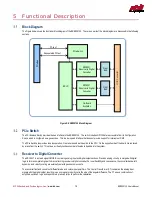
Страница 19: ...ards to be added to the system Resolver to Digital Converter The RD 19231 is a mixed signal CMOS IC containing analog input and digital output sections Precision analog circuitry is merged with digita...

Страница 20: ...Hz 1200 rpm High Velocity 2 0 10 kHz 12 bit Synchro Resolver 10 bit LVDT 750 Hz 19200 rpm Front End The front end consists of a precision resistor pack that sets the input voltage range 2V 11 8V or 90...

Страница 21: ...S2 for positive and S4 for negative This section described how to connect and configure this board for use with a resolver A resolver also requires a reference input Please see Section 6 2 on page 26...

Страница 22: ...see Section 6 2 on page 26 for information on connecting the reference Input Connections Table 10 Synchro Input Connections Sensor ERES35105 IDAN ERES35105 Lead Description Pin Name Channel 0 Pin Cha...

Страница 23: ...ilitate this the signal path allows the addition of gain Contact RTD Tech Support for more details Figure 9 2 Wire LVDT Schematic Input Connections Table 12 2 Wire LVDT Input Connections Sensor ERES35...

Страница 24: ...Contact RTD Tech Support for more details Figure 10 3 Wire LVDT Schematic Input Connections Table 14 3 Wire LVDT Input Connections Sensor ERES35105 IDAN ERES35105 Lead Description Pin Name Channel 0 P...

Страница 25: ...IDAN ERES35105 Lead Description Pin Name Channel 0 Pin Channel 1 Pin Channel 0 Pin Channel 1 Pin No Connection CHx_S1 19 27 10 14 No Connection CHx_S2_RESOLVER 23 31 12 16 No Connection CHx_S2_SYNCHRO...

Страница 26: ...VDT mode the reference is derived on board from the input signals The CHx_REF_IN signals must be left unconnected 6 2 1 INTERNALLY GENERATED REFERENCE Connections Table 18 Internal Reference Connectio...

Страница 27: ...ion JP119 JP219 1 2 JP120 JP220 2 3 2VRMS 1 2 11 8VRMS Open 90VRMS JP121 JP221 2 3 2VRMS 1 2 11 8VRMS Open 90VRMS JP122 JP222 1 2 6 2 3 SINGLE ENDED EXTERNALLY GENERATED REFERENCE Connections Table 22...

Страница 28: ...fying the ERES35105 Configuration Space Offset Register Description Value 0x00 Vendor ID 0x104C 0x02 Device ID 0x8232 0x84 Subsystem Vendor ID 0x1435 0x86 Subsystem ID 0x3616 Index and Data Registers...

Страница 29: ...e Index Register a Set SELECT such that DATA 0 WR_STRB 0 and OE 1 and set INDEX_DATA to the desired Index b Set GPIOAB_CTRL and GPIOCD_CTRL to their Write values c Set SELECT such that DATA 0 WR_STRB...

Страница 30: ...t INDEX_DATA to the desired Index again 4 Set the Data Register a Set SELECT such that DATA 1 WR_STRB 0 and OE 1 and set INDEX_DATA to the desired Data b Set GPIOAB_CTRL and GPIOCD_CTRL to their Write...

Страница 31: ...DATA with the WR_STRB bit cleared to make sure a write isn t duplicated NOTE If multi thread safe operation is not required steps 1 and 3 can be eliminated Board Registers Table 26 Board Registers Ind...

Страница 32: ...ead Write Selects the bandwidth filter See Section 5 3 1 on page 20 0 Filter 2 High Velocity 1 Filter 1 High Resolution B1 DN_UP Read Write 0 Inactive bandwidth filter is precharged with a gain of 4 R...

Страница 33: ...TA_IN register as the Read Data 7 5 2 CHANNEL X MODE 0X00 AND 0X02 This shift register select line is connected to an Intersil ISL22424 digital potentiometer The H pin which corresponds to a wiper val...

Страница 34: ...is used to trim the velocity gain of the control loop Wiper 1 of the potentiometer is used to trim the velocity offset of the control loop Velocity trimming is only required when using the analog CHx_...

Страница 35: ...f the potentiometer is used to adjust the amplitude of the Channel 0 Excitation Wiper 1 of the potentiometer is used to adjust the amplitude of the Channel 1 Excitation Output Data The Table below sho...

Страница 36: ...stem to see if there is a specific module that is causing a problem Perform you troubleshooting with the least number of modules in the system possible Swap Components Try replacing parts in the syste...

Страница 37: ...pecifications A copy of the latest PC 104 specifications can be found on the webpage for the PC 104 Embedded Consortium www pc104 org PCI and PCI Express Specification A copy of the latest PCI and PCI...

Страница 38: ...other contingencies beyond the control of RTD Embedded Technologies or as a result of service or modification by anyone other than RTD Embedded Technologies Except as expressly set forth above no oth...

Страница 39: ...ologies Inc 103 Innovation Boulevard State College PA 16803 USA Telephone 814 234 8087 Fax 814 234 5218 www rtd com sales rtd com techsupport rtd com Copyright 2019 by RTD Embedded Technologies Inc Al...

Отзывы: