RTD Embedded Technologies, Inc.
|
www.rtd.com
28
ERES35105
User’s Manual
7
Register Address Space
The bus interface is provided through the GPIO of the PCIe Switch. The GPIO are configured as a generic bus, and the board registers are
accessed through an index and data register. The following sections describe the steps needed to access the board registers.
NOTE: It may be necessary to disable PCIe Active State Power Management
(ASPM) in the BIOS setup utility for correct operation. This is typically
in the “Advanced/PCI Express/Port #” menu. Contact your CPU
vendor for details.
Identifying the Board
The ERES35105 shows up in standard PCI Configuration space as a set of PCI to PCI Bridges. It can be positively identified as shown in the
Table below.
Table 24: Identifying the ERES35105
Configuration
Space Offset
Register Description
Value
0x00
Vendor ID
0x104C
0x02
Device ID
0x8232
0x84
Subsystem Vendor ID
0x1435
0x86
Subsystem ID
0x3616
Index and Data Registers
Table 25: Index and Data Registers
Configurat
ion Space
Offset
0x03
0x02
0x01
0x00
0xBC
GPIOAB_CTRL
0xC0
GPIOCD_CTRL
0xC4
SELECT
INDEX_DATA
7.2.1
GPIOAB_CTRL
(R
EAD
/W
RITE
)
This register is used to set the direction for the GPIO port. The values to write to it are:
0x12491249 for a Write operation
0x00000000 for a Read operation
7.2.2
GPIOCD_CTRL
(R
EAD
/W
RITE
)
This register is used to set the direction for the GPIO port. The values to write to it are:
0x01491249 for a Write operation
0x01480000 for a Read operation
7.2.3
SELECT
(R
EAD
/W
RITE
)
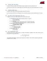
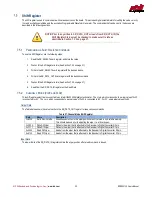
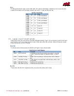
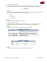
This register is used to select between the Index and Data register. All undefined bits may be written with a 0.
B2: DATA
0 = Accessing Index register
1 = Accessing Data register
B1:WR_STRB
Writes take effect on 0 to 1 transition

