background image

Rastergraf


3-34  Connector Pinouts and Cable Information 


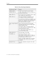
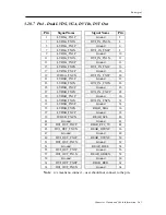
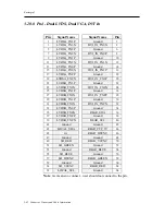
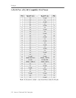
Table 3-24  Rear Panel Signal Definitions  

Pn4/Schematic Name 

Function 

LVDSA_TX3P, 
LVDSB_TX3P, etc. 

LVDS Ch A and Ch B (respectively) signals. 
LVDSA_TX3P/ LVDSA _TX3N would make up a 
high-speed differential pair.  

DVID_TXCP, etc. 
 
DVIB_TXCP, etc. 


DVI In signals. DVID_TXCP/DVID_TXCN would 
make up a high-speed differential pair. 
DVI Out signals. DVIB_TXCP/DVIB_TXCN 
would make up a high-speed differential pair. 
Note that all lines must be the same length and each 
pair must use twisted pair with shield cabling. Each 
shield must be separately tied to ground, not all 
shields together and then to ground. 

REAR_ VIN3/HS_HSYNC

etc. 

This is a signal pin shared between the Bt835 
NTSC/PAL/SECAM decoder and the high-speed 
AD9882 RGBHV decoder. 
VIN indicates a Bt835 video input multiplexer 
input. Numeral indicates which physical port. VIN3 
would be the fourth (0-3) input. 
HS_ means high-speed signal. HSYNC is, of 
course, horizontal sync input. 

REAR_GREEN

, etc. 

SO_GREEN, etc. 

Part of the Primary VGA output.   
Part of the Secondary VGA output.   
RED, GREEN, and BLUE must use 75-ohm coax. 
Each shield must be separately tied to ground, not 
all shields together and then to ground. 
HSYNC and VSYNC should each be twisted pair 
with a ground. SDC and SDA can be straight or 
twisted pairs. 

REAR_COUT

, etc. 

Part of the component or composite video output 
signal set. 


Содержание Duros

Страница 1: ...Topaz Stratus Tropos Garnet and Duros PMC Graphics Boards User s Manual Rastergraf Inc 1810 J SE First St Redmond OR 97756 541 923 5530 web http www rastergraf com Release 3 7 May 7 2017 Rastergraf...

Страница 2: ...REFERENCES 1 27 CHAPTER 2 SPECIFICATIONS 2 1 2 1 GENERAL 2 2 2 2 SPECIFICATIONS UNIQUE TO TOPAZ STRATUS AND GARNET 2 8 2 3 DISPLAY TIMING 2 10 2 4 MONITOR REQUIREMENTS 2 12 2 5 VERIFIED DISPLAY AND C...

Страница 3: ...39 3 20 6 Pn4 Dual LVDS Dual VGA Analog Video I O 3 40 3 20 7 Pn4 Dual LVDS VGA DVI In DVI Out 3 41 3 20 8 Pn4 Dual LVDS Dual VGA DVI In 3 42 3 20 9 Pn4 Dual LVDS Single VGA 3 43 3 20 10 Pn4 RG 101 C...

Страница 4: ...2 C 5 20 5 7 TOPAZ STRATUS GARNET AUXILIARY REGISTER 5 21 5 8 DVI DIGITAL VIDEO OUTPUT 5 22 5 9 ADV7123 AND ADV7120 VGA DACS 5 24 5 10 AD9882 HIGH SPEED DIGITIZER STRATUS GARNET 5 25 5 11 BT835 NTSC P...

Страница 5: ...D2 3 8 Table 3 6 Video I O VI O Front Panel Connector Pinouts 20A 20B 3 9 Table 3 7 Video I O VI O Front Panel Connector Pinouts 26A 26C 3 11 Table 3 8 Video I O VI O Front Panel Connector Pinouts MDS...

Страница 6: ...17 Front and Rear Panel I O Options for Stratus 1 23 Figure 1 18 Front and Rear Panel Output Options for Tropos 1 23 Figure 1 19 Rear Panel I O Options for Garnet 1 24 Figure 1 20 Rear Panel Output Op...

Страница 7: ...PV3060 4 13 Figure 4 8 Installation of a PMC Module onto a PCI PMC Carrier 4 15 Figure 4 9 Installation of a PCI Module into an Emerson MTX 4 16 Figure 4 10 Installation of a PMC Module onto a 3U CPCI...

Страница 8: ......

Страница 9: ...to six chapters Chapter 1 General Information Chapter 2 Specifications Chapter 3 Connector Pinouts and Cable Information Chapter 4 Installing Your Graphics Board Chapter 5 Programming Devices and Memo...

Страница 10: ...If your problem is monitor related Rastergraf technical support will need detailed information about your monitor Board Revisions This manual applies to the following board revision levels Tropos Str...

Страница 11: ...hich can cause radio interference Rastergraf Inc assumes no liability for any damages caused by such interference Rastergraf Inc s products are not authorized for any use as critical components in fli...

Страница 12: ...mmands Commands in code fragments are preceded by the system prompt a percentage sign the standard prompt in UNIX s C shell or the hash mark the standard UNIX prompt for the Super User Keyboard usage...

Страница 13: ...Rastergraf General Information 1 1 Chapter 1 General Information...

Страница 14: ...s the Topaz a non conduction cooled design which is intended to subsume the Stratus and Tropos It a includes the new features added in the Garnet and Duros b using an MDR26 connector adds the optional...

Страница 15: ...ont rear yes rear only rear only MDR26 LVDS front panel connector option yes n a n a Single DVI options front rear yes yes yes Composite S Video output yes yes yes MDSM 16 Video I O connector no Strat...

Страница 16: ...nput Processor THine THC63DV164 DVI Output Encoder BIOS EEPROM LVDS Out Video Out Video In DVI In RGB In Ch 1 Ch 2 Select VGA Ch 1 Out DVI Out 32 bit 33 66 MHz Silicon Motion SM731 Graphics Accelerato...

Страница 17: ...ltiplexer Analog Devices AD9882 High Speed RGB DVI Digitizer Conexant Bt835 Video Input Processor THine THC63DV164 DVI Output Encoder BIOS EEPROM LVDS Out Video Out Video In DVI In RGB In Ch 1 Ch 2 Se...

Страница 18: ...cessor 235 MHz RAMDAC NTSC PAL Video Encoder Flat Panel Drivers Dual Channel LVDS Encoder BIOS Memory Interface I 2 C Controller PLD Controller I O Resource Manager THine THC63DV164 DVI Output Encoder...

Страница 19: ...face I 2 C Controller PLD Controller I O Resource Manager PLD for YUV RGB Multiplexer Analog Devices AD9882 High Speed RGB DVI Digitizer Conexant Bt835 Video Input Processor THine THC63DV164 DVI Outpu...

Страница 20: ...ideo Encoder Flat Panel Drivers Dual Channel LVDS Encoder BIOS Memory Interface I 2 C Controller PLD Controller I O Resource Manager PLD for STANAG THine THC63DV164 DVI Output Encoder BIOS EEPROM LVDS...

Страница 21: ...n This level of power management is possible since each functional block and engine clock can be dynamically controlled to actively reduce the overall power consumption Figure 1 6 SM731 Application Bl...

Страница 22: ...64 bit memory bus operating at up to 150 MHz The 1 2 GB sec peak bandwidth available allows concurrent support of large displays and other processing functions at optimum performance SM731 can drive...

Страница 23: ...ntegrated Dual Channel LVDS transmitters with DualMon support QuickRotate feature for instantaneous rotation On Chip Dual Display Support RGB VIDEO NTSC PAL LVDS RGB VGA LVDS LVDS and LVDS VIDEO Video...

Страница 24: ...site RGB to YUV Encoding Matrix Clock Generation Timing Control Modulators Y U V Luma trap 16 MB On Chip Memory for Capture Buffer and Frame Buffer Capture Engine 2D 3D 128 bit Graphics Engine Memory...

Страница 25: ...capture support from NTSC PAL rate and RGBHV or DVI up to SXGA enabling real time full frame rate display of live video as well as frame grabber functionality that can upload images to the host Video...

Страница 26: ...ted into the graphics display without introducing video related artifacts Figure 1 9 Capture Buffer and Display Memory Video Playback Once the incoming digitized video data has been placed into the ca...

Страница 27: ...t a later time Alternatively the host CPU can perform a color space transform on the YUV data or extract the luminance in order to generate an 8 bit gray scale image Image enhancement algorithms may b...

Страница 28: ...put Hue saturation brightness and contrast controls provide added flexibility to enhance the appearance of the decoded image Cropping and scaling can shrink the input image to no more than is needed f...

Страница 29: ...G applications The AD9882 also contains a DVI 1 0 compatible receiver and supports display resolutions up to SXGA 1280 x 1024 at 60 Hz The receiver operates with true color 24 bit panels and also feat...

Страница 30: ...hermore the LCD panels can be programmed to display images from either controller with some restrictions The Digital Interface can drive data from either the Panel Controller or the CRT Controller jus...

Страница 31: ...DVI output pins The secondary VGA DAC port is driven by the Flat Panel display controller section of the SM731 Displays ranging up to 1024 x 768 are practical when both channels are active Some screen...

Страница 32: ...r optic cables Displays ranging up to 1600 x 1200 are supported when best quality cables are used The DVI serializer is driven by the Flat Panel display controller section of the SM731 Three TMDS data...

Страница 33: ...4 bpp panels and if used in conjunction with the LVDS2 Interface it can be used to drive a two channel two pixels per clock panel of up to QXGA size 2048x1536 Figure 1 15 LVDS Flat Panel Output Block...

Страница 34: ...ssible both to front panel connectors as well as the rear panel I O Pn4 connector Figure 1 16 Front and Rear Panel I O Options for Topaz Jumper Networks Connectors RP16 18 0 ohm Network RP53 0 ohm Net...

Страница 35: ...2 Analog Video In and SM731 Video Out THine THC63DV164 DVI Encoder Jumper Networks ADV7123 RGB DAC Secondary VGA DVI Connector DVI pins Rear Panel DVI pins RP60 0 ohm Network DVI Connector Spare pins...

Страница 36: ...RP51 0 ohm Network RP55 0 ohm Network Bt835 AD9882 Analog Video In and SM731 Video Out THine THC63DV164 DVI Encoder Jumper Networks Rear Panel DVI pins RP63 0 ohm Network RP62 0 ohm Network Rear Panel...

Страница 37: ...for VxWorks and Linux VxWorks WindML layered on top of SDL Built in Test BIT routines callable by CPU layered on top of SDL 1 9 Additional Details About SDL SDL is a graphics library designed to be a...

Страница 38: ...tipple patterns Complete information about SDL is contained in the Standard Drawing Library C Reference Manual that is available for download from our web site at http www rastergraf com SDL Feature S...

Страница 39: ...id 54 THine THC63DV164 DVIencoder Contact Rastergraf support rastergraf com Analog Devices AD9882 RGB YUV DVI Digitizer and ADV7123 DAC AD9882 http www analog com en prod 0 765_806_AD9882A 2C00 html A...

Страница 40: ......

Страница 41: ...Rastergraf Specifications 2 1 Chapter 2 Specifications...

Страница 42: ...Green and Blue 5 5 5 or 5 6 5 For 24 bpp pixel is divided into Red Green and Blue and the data is ordered as packed pixels in memory Scroll Pan and Zoom Scroll single line smooth scroll Pan anywhere...

Страница 43: ...ture Coefficient PTC resistor It resets automatically when an overload is removed PCI Bus Access Programmable Bus Address Registers BARs in the SM731 map control and drawing engine registers and displ...

Страница 44: ...esolution displays and as much other simultaneous activity as possible Testing Conditions Windows 2000 dual display format is 1280 x 1024 x 32 bpp Cautionary Note Your mileage may vary It would be pru...

Страница 45: ...CCPMC form factor compatible This is primarily intended to allow the boards to be used in applications that might require a display board for debugging purposes in system development The Garnet and D...

Страница 46: ...aids available from Rastergraf that might be used as part of a rear panel system integration effort Ruggedization Option Rastergraf is not in the militarized business but it does offer ruggedized ver...

Страница 47: ...0 to 100 condensing 0 to 100 condensing 0 to 100 condensing Vibration Sine 1 2 g peak 15 2 kHz 2 g peak 15 2 kHz 10 g peak 15 2 kHz 10 g peak 15 2 kHz 10 g peak 15 2 kHz 10 g peak 15 2 kHz Vibration...

Страница 48: ...GA DAC and a THine THC63DV164 DVI encoder Thus depending on the user requirements the FP port can either supply a DVI encoded single channel graphics out or the second VGA port When used in the second...

Страница 49: ...uminance component can be forced to 0x80 yielding monochrome Analog Interface 140 MSPS Maximum Conversion Rate Programmable Analog Bandwidth 0 5 V to 1 0 V Analog Input Range 500 ps p p PLL Clock Jitt...

Страница 50: ...Active Display VESA Format Bits per Pixel Vertical Refresh Horizontal Refresh Pixel Clock 640 x 480 n a VGA VGA VGA 8 16 32 60 Hz 72 Hz 75 Hz 85 Hz 31 5 kHz 37 9 kHz 37 5 kHz 43 4 kHz 25 175 MHz 31 5...

Страница 51: ...al Refresh Pixel Clock 640 x 480 Both VGA 8 16 32 75 Hz 37 65 kHz 30 72 MHz 800 x 600 Both SVGA 8 16 32 75 Hz 47 03 kHz 48 90 MHz 1024 x 768 Both UVGA 8 16 32 75 Hz 60 15 kHz 81 80 MHz 1152 x 900 Anal...

Страница 52: ...nization High bandwidth 135 MHz at 1280 x 1024 180 MHz at 1600 x 1200 Horizontal refresh rate 70 kHz at 1280 x 1024 90 kHz at 1600 x 1200 See Section 2 3 for complete display timing information Notes...

Страница 53: ...means FP timing used for VGA out Mode VP in DVI column means VP timing used for DVI out TV in VGA column means scaled TV out used instead of RGB out Window is 640x488 YUV422 values are N no Y Window...

Страница 54: ...Y Y snow OK 1280 32 1280 16 N N Y Y OK OK 1280 32 1280 16 CAP N Y Y light snow light snow 1280 32 1280 16 N CAP Y Y light snow light snow 1280 32 1280 32 N CAP N N light snow snow in window 1280 32 1...

Страница 55: ...ne running during these tests It may be that the display could be acceptable at higher rates because we rejected any noticeable artifacts even tiny amounts of snow But as mentioned before differences...

Страница 56: ...ng engine was not active Table 2 6 Maximum Display Capture Format Capabilities DVI mode VGA mode DVI Window VGA Window 1600 8 63 VGA DVI 1024 75 VGA DVI 1600 8 73 VGA DVI 640 60 VGA DVI 1600 8 77 VGA...

Страница 57: ...signal sets simultaneously Tropos and Topaz on board 3 3V regulator for backplanes which do not have 3 3V The Topaz Stratus Garnet graphics board includes the Topaz Tropos Duros with DVI features abo...

Страница 58: ...31 00735 5012 20B D1 DVI I DVI I DVI I PMC Pn4 PMC Pn4 MDR20 TopazPMC 2L VGA A31 00735 2012 MDR A31 00735 8012 26A VGA 1 PMC Pn4 MDR26 MDR26 MDR26 TopazPMC 2N VGA A31 00735 2012 MDR A31 00735 7012 26B...

Страница 59: ...up 5 StratusPMC RIO3 GarnetPMC RIO6 TopazPMC 2R4 DVI In or Analog RGB In 3 20 5 Pn4 Pin Group 1 Pn4 Pin Group 3 Pn4 Pin Group 2 Pn4 Pin Group 4 Pn4 Pin Group 5 StratusPMC RIO4 GarnetPMC RIO7 TopazPMC...

Страница 60: ...Sales for special requirements Table 2 10 Software Operating System Software Linux VxWorks Windows 2000 XP LynxOS 4 X Window System XFree86 4 3 XFree86 4 3 XFree86 4 3 Video Input Extension bttv bttv...

Страница 61: ...Rastergraf Connector Pinouts and Cable Information 3 1 Chapter 3 Connector Pinouts and Cable Information...

Страница 62: ...unused DVI dual link pins secondary VGA The Topaz Stratus MDSM or MDR20 Video I O breakout cable splits out video in and out into BNC and or S Video connections The Garnet and Duros use only PMC Pn4...

Страница 63: ...t all shields together and then to ground VIN3 HS_HSYNC etc This is a signal pin shared between the Bt835 NTSC PAL SECAM decoder and the high speed AD9882 RGBHV decoder VIN indicates a Bt835 video inp...

Страница 64: ...C 2A 2M S Video Adapters 3 10 DVI I VGA A31 00735 1012 D2 Topaz Stratus Tropos Multifunction Breakout Cable 3 11 DVI VGA 88741 8700 A31 00599 5012 D1 TopazPMC 1D StratusPMC 1D StratusPMC 2x TroposPMC...

Страница 65: ...stergraf for assistance The R G and B video outputs are driven by the SM731 graphics controller chip which is capable of driving terminated cable 75 ohms to standard RS 330 IRE levels Cable length sho...

Страница 66: ...nd 6 Red Ground Circuit Ground 7 Green Ground Circuit Ground 8 Blue Ground Circuit Ground 9 Fused 5 Volts 25A max 10 Sync Ground Circuit Ground 11 Ground Circuit Ground 12 DDCDA Twisted Pair with pin...

Страница 67: ...losely matched in length Note that there is only one DVI channel It is driven by an external DVI encoder connected the SM731 24 bit FP channel output The encoder is a THine THC63DV164 DVI transmitter...

Страница 68: ...le below shows the usage of the DVI I pins for the TopazPMC 2 and StratusPMC Non standard usages are shown in bold italic Table 3 5 TopazPMC 2 and StratusPMC DVI I Connector Pinout D2 DVI I Pin Descri...

Страница 69: ...8 10 18 20 n c n c 3 4 1 MDR20 Pinout 20A NTSC PAL or RGBHV In NTSC PAL Out The MDR20 Pinout 20A supports dual use pins The NTSC PAL and high speed RGB input signals are connected together on the boa...

Страница 70: ...0A pin definitions share pins between the NTSC PAL digitizer and the high speed digitizer The connections are wired in parallel except for that the 75 ohm terminations on VIN3 and CIN are removed in H...

Страница 71: ...VDSB_TX1P 18 CIN HS_VSYNC DVI_IN_TX2P FLVDSB_TX1N 6 VIN2 HS_BLUE DVI_IN_ TX0P FLVDSB_TX0P 19 VIN3 HS_HSYNC DVI_IN_ TX0N FLVDSB_TX0N 7 Ground Ground Ground 20 F5V F5V F5V 8 FLVDSA_TX3P FLVDSA_TX3P FLVD...

Страница 72: ...HV or RGB SOG up to 1280 x 1024 at 120 MHz The table above shows the MDR26 Pinout 26A pin definitions share pins between the NTSC PAL digitizer and the high speed digitizer The connections are wired i...

Страница 73: ..._IN_TX2N 4 CIN HS_VSYNC DVI_IN_TX2P 5 YIN_VIN0 HS_RED DVI_IN_ TX1P 6 VIN1 HS_GREEN DVI_IN_ TX1N 7 VIN2 HS_BLUE DVI_IN_ TX0P 8 VIN3HS_HSYNC DVI_IN_ TX0N 9 Ground Ground 10 14 Ground Ground Factory opti...

Страница 74: ...acquires RGBHV or RGB SOG up to 1280 x 1024 at 120 MHz The table above shows the Pinout MDSMA pin definitions share pins between the NTSC PAL digitizer and the high speed digitizer The connections are...

Страница 75: ...video in because it is the most common type and is also widely used on PCs and personal video equipment This makes it easy to get cables and connectors Figure 3 1 S Video Connector Pin Description 1 G...

Страница 76: ...Cable A31 00599 1012 Figure 3 2 VGA to VGA Extension Cable A31 00599 1012 VGA P1 VGA C2 Wire Description Pin Pin Type Function Name 2 2 75 coax G VGA Green 7 7 75 coax G VGA Green Ground 3 3 75 coax...

Страница 77: ...pin on the input S Video cable can be used as a standard composite input The A31 00709 1003 S Video to BNC adapter cable is supplied for that purpose Table 3 10 TopazPMC S Video to BNC adapter cable A...

Страница 78: ...YOUT COUT to S Video adapter can be used to provide S Video Input and Output connections Table 3 11 StratusPMC BNC to S Video Adapter Cable VAD44 BNC BNC S Video Wire Description Pin Connector Pin Ty...

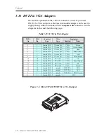
Страница 79: ...ions Using spare pins on the DVI I connector it provides extra signal sets including DVI and Primary and Secondary VGA Note that there is only one DVI channel It is driven by an external DVI encoder c...

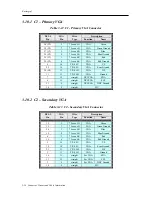
Страница 80: ...H VGA HS 11 11 TP S H VGA Ground 7 12 straight DVI VGA SDA 6 15 straight DVI VGA SCL 11 5 straight DVI VGA DDC Ground 14 9 straight F5V 3 10 2 C2 Secondary VGA Table 3 13 C2 Secondary VGA Connector D...

Страница 81: ...aight DVI VGA SDA 6 6 straight DVI VGA SCL 14 14 straight F5V 23 23 TP S C DVI DVIC_TXCLKP 24 24 TP S C DVI DVIC_TXCLKN 22 22 TP S C DVI Pair DCK Ground 18 18 TP S 0 DVI DVIC_TX0P 17 17 TP S 0 DVI DVI...

Страница 82: ...on Pin Pin Type Type Function Name 2 2 female VGA 75 coax G VGA Green 7 7 female VGA 75 coax G VGA Green Ground 3 3 female VGA 75 coax B VGA Blue 8 8 female VGA 75 coax B VGA Blue Ground 1 1 female VG...

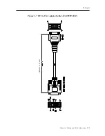
Страница 83: ...Rastergraf Connector Pinouts and Cable Information 3 23 Figure 3 7 DVI to VGA Adapter Cable A31 00599 5012 305 mm 12 mm...

Страница 84: ...Pin Pin Type Type Function Name 2 2 female VGA 75 coax G VGA Green 7 7 female VGA 75 coax G VGA Green Ground 3 3 female VGA 75 coax B VGA Blue 8 8 female VGA 75 coax B VGA Blue Ground 1 1 female VGA...

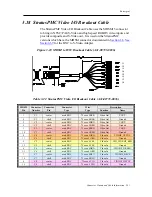
Страница 85: ...ell female BNC 75 coax GRN Video In Ground 6 C7 center female BNC 75 coax BLU Video In VIN2 HS_BLUE 4 C7 shell female BNC 75 coax BLU Video In Ground 16 C8 center female BNC 75 coax VIO Video In VIN3...

Страница 86: ...connector documented in Section 3 4 Table 3 18 TopazPMC DVI In Adapter Cable MDR20 DVI D Wire Description Pin Pin Type Function Name 12 23 TP S C DVI DVID_TXCLKP 2 24 TP S C DVI DVID_TXCLKN 1 22 TP S...

Страница 87: ...le BNC 75 coax BRN Video Out Ground 3 C54 3 female S Video In 75 coax YEL Video In YIN_VIN0 HS_RED 1 C54 1 female S Video In 75 coax YEL Video In Ground 18 C54 4 female S Video In 75 coax ORG Video In...

Страница 88: ...1P 16 C1 9 female DVI D TP S 1 DVI DVID_TX1N 14 C1 11 female DVI D TP S 1 DVI Pair D1 Ground 5 C1 2 female DVI D TP S 2 DVI DVID_TX2P 18 C1 1 female DVI D TP S 2 DVI DVID_TX2N 4 C1 3 female DVI D TP S...

Страница 89: ...azPMC 1L version which has the MDR26 connector documented in Section 3 5 The cable is the same as the 3M 14B26 SZLB 300 0LC 3 meter with thumbscrews cable Note that the connections are not the same at...

Страница 90: ...Pair BL1 Ground 6 21 Male MDR26 TP S B0 LVDS Out FLVDSB_TX0P 19 8 Male MDR26 TP S B0 LVDS Out FLVDSB_TX0N 13 14 Male MDR26 TP S B0 LVDS Out Pair BL0 Ground 7 20 Male MDR26 TP S C0 Term 100 ohm term P...

Страница 91: ...le BNC 75 coax BLK Video Out YOUT 9 C1 shell male BNC 75 coax BLK Video Out Ground 2 C2 center male BNC 75 coax BRN Video Out VOUT 9 C2 shell male BNC 75 coax BRN Video Out Ground 3 C3 center male BNC...

Страница 92: ...ction Name 1 24 female DVI D 75 coax BLK Video Out DVID_TXCLKN 2 23 female DVI D 75 coax BRN Video Out DVID_TXCLKP 9 22 female DVI D 75 coax BRN Video Out Ground 3 1 female DVI D 75 coax RED Video Out...

Страница 93: ...os or Stratus i e without the rear panel I O option LVDS will still be on Pn4 While using Pn4 I O is very attractive for some applications there can be some serious difficulties in successfully deploy...

Страница 94: ...ed to ground not all shields together and then to ground REAR_ VIN3 HS_HSYNC etc This is a signal pin shared between the Bt835 NTSC PAL SECAM decoder and the high speed AD9882 RGBHV decoder VIN indica...

Страница 95: ...4 25 Ground C BE3L 26 27 AD22H AD21H 28 29 AD19H VCC 5V 30 31 byp Vio AD17H 32 33 FRAMEL Ground 34 35 Ground IRDYL 36 37 DEVSELL VCC 5V 38 39 Ground n c 40 41 n c n c 42 43 PAR Ground 44 45 byp Vio AD...

Страница 96: ...Ground 18 19 AD30H AD29H 20 21 Ground AD26H 22 23 AD24H VDD 3 3V 24 25 IDSEL AD23H 26 27 VDD 3 3V AD20H 28 29 AD18H Ground 30 31 AD16H C BE2L 32 33 Ground n c 34 35 TRDYL VDD 3 3V 36 37 Ground STOPL 3...

Страница 97: ...8 19 LVDSA_TXCN n c 20 21 LVDSB_TX3P Ground 22 23 LVDSB_TX3N n c 24 25 LVDSB_TX2P Ground 26 27 LVDSB_TX2N n c 28 29 LVDSB_TX1P Ground 30 31 LVDSB_TX1N n c 32 33 LVDSB_TX0P Ground 34 35 LVDSB_TX0N n c...

Страница 98: ...22 23 LVDSB_TX3N n c 24 25 LVDSB_TX2P Ground 26 27 LVDSB_TX2N n c 28 29 LVDSB_TX1P Ground 30 31 LVDSB_TX1N n c 32 33 LVDSB_TX0P Ground 34 35 LVDSB_TX0N n c 36 37 LVDSB_TXCP Ground 38 39 LVDSB_TXCN n...

Страница 99: ...DSB_TX3P Ground 22 23 LVDSB_TX3N REAR_COUT 24 25 LVDSB_TX2P Ground 26 27 LVDSB_TX2N REAR_VOUT 28 29 LVDSB_TX1P Ground 30 31 LVDSB_TX1N REAR_YOUT 32 33 LVDSB_TX0P Ground 34 35 LVDSB_TX0N REAR_SDA 36 37...

Страница 100: ...REAR_ CIN HS_VSYNC 20 21 LVDSB_TX3P Ground 22 23 LVDSB_TX3N REAR_COUT 24 25 LVDSB_TX2P Ground 26 27 LVDSB_TX2N REAR_VOUT 28 29 LVDSB_TX1P Ground 30 31 LVDSB_TX1N REAR_YOUT 32 33 LVDSB_TX0P Ground 34 3...

Страница 101: ...23 LVDSB_TX3N DVI_IN _TX2N 24 25 LVDSB_TX2P Ground 26 27 LVDSB_TX2N DVI_IN _TXCP 28 29 LVDSB_TX1P Ground 30 31 LVDSB_TX1N DVI_IN _TXCN 32 33 LVDSB_TX0P Ground 34 35 LVDSB_TX0N REAR_SDA 36 37 LVDSB_TXC...

Страница 102: ...SB_TX3P Ground 22 23 LVDSB_TX3N DVI_IN _TX2N 24 25 LVDSB_TX2P Ground 26 27 LVDSB_TX2N DVI_IN _TXCP 28 29 LVDSB_TX1P Ground 30 31 LVDSB_TX1N DVI_IN _TXCN 32 33 LVDSB_TX0P Ground 34 35 LVDSB_TX0N REAR_S...

Страница 103: ...21 LVDSB_TX3P Ground 22 23 LVDSB_TX3N n c 24 25 LVDSB_TX2P Ground 26 27 LVDSB_TX2N n c 28 29 LVDSB_TX1P Ground 30 31 LVDSB_TX1N n c 32 33 LVDSB_TX0P Ground 34 35 LVDSB_TX0N REAR_SDA 36 37 LVDSB_TXCP...

Страница 104: ...8 19 n c n c 20 21 n c Ground 22 23 n c n c 24 25 n c Ground 26 27 n c n c 28 29 n c Ground 30 31 n c n c 32 33 n c Ground 34 35 n c n c 36 37 n c Ground 38 39 n c n c 40 41 Ground Ground 42 43 REAR_H...

Страница 105: ...Rastergraf Installing Your Rastergraf Graphics Board 4 1 Chapter 4 Installing Your Rastergraf Graphics Board...

Страница 106: ...information regarding repair or replacement Do not attempt to use damaged equipment Caution Be careful not to remove the board from its antistatic bag until you are ready to install it It is preferab...

Страница 107: ...S and or BIOS while booting up there aren t any address jumpers The address settings are programmable and are set up by the software as a result of information supplied by the OS at boot time Refer to...

Страница 108: ...board In other words if you need to have two graphics boards in the system they both or neither have to be Rastergraf boards If your CPU chip set has a built in graphics adapter and you want to run Wi...

Страница 109: ...11 C6 C 165 C163 R 14 R 57 L1 C146 R61 R 13 L8 C143 C144 C147 R 63 C145 C164 RP56 RP63 VR 8 R8 U8 R6 R59 C 20 R 56 R54 R5 R P52 RP60 RP53 R 71 R 70 C 80 R P62 RP50 R P51 D PAC K5 R P61 D PAC K2 R58 C5...

Страница 110: ...for the Fab Rev 1 TopazPMC Board JP4 JP2 JP1 JP3 DVI I Connector Primary VGA Connector Secondary Connect PMC J4 Connector MDR20 Connector MDR26 Connector Not all connectors can be installed at the sa...

Страница 111: ...for the Fab Rev 2 TopazPMC Board JP4 JP1 JP2 JP3 DVI I Connector Primary VGA Connector Secondary Connect PMC J4 Connector MDR20 Connector MDR26 Connector Not all connectors can be installed at the sa...

Страница 112: ...L11 C165 C 163 L8 C 146 C20 R 5 C143 C147 C 145 C164 C 144 C 29 C 17 RP53 R 53 R P62 R 54 R13 L3 U 8 R 3 RP50 R P 61 F2 RP51 C 114 C 58 C65 D PAC K1 C 133 VR 4 L2 R 2 C 14 R 9 R 21 C69 C79 C41 R68 C14...

Страница 113: ...R70 C 184 R71 C187 C185 L5 C31 C8 C148 C37 C42 R41 R33 L4 C36 R 4 C28 R P56 R 6 C35 R 1 R 8 L9 R 108 U11 L11 C6 U302 C131 C165 R14 C163 R 61 L1 C146 L8 R105 R13 R 63 C143 C144 C147 C 145 C164 C20 R10...

Страница 114: ...will not work reliably at 66 MHz Unless you are certain that your system is running and will always be run only at 33 MHz you must use an active on board bridge PCI or CompactPCI carrier 33 MHz 66 MH...

Страница 115: ...an exist in the equipment 2 Open the computer and remove the CPU board onto which the graphics PMC board is to be installed Identify an empty PMC location generally there are one or two on a given CPU...

Страница 116: ...Rastergraf 4 12 Installing Your Rastergraf Graphics Board Figure 4 6 Installation of a PMC Module into an Emerson MVME2604...

Страница 117: ...he mounting screws two near the front and two near the PMC connectors Note Sometimes the graphics board front panel can hang up going into the carrier front panel hole This can be because there is a l...

Страница 118: ...sure that the carrier is correctly configured to supply local 3 3V Installation Procedure 1 Shut down the operating system and turn off the power Warning Never open the computer without turning off t...

Страница 119: ...tatic electricity that your body builds up normally can seriously damage the components on the graphics board 3 Wear a grounded wrist strap and touch a metal part of the computer chassis Remove the ca...

Страница 120: ...e 4 9 Installation of a PCI Module into an Emerson MTX 4 After making sure the board is seated correctly install the screw into the place where the blocking plate was and which now holds the graphics...

Страница 121: ...cord plugged in so as to ground the computer chassis You can easily get shocked ruin computer parts or both unless you turn off the power Even with power switched off lethal voltages can exist in the...

Страница 122: ...3U CPCI PMC Carrier Caution The static electricity that your body builds up normally can seriously damage the components on the graphics board 3 Wear a grounded wrist strap Touch a metal part of the c...

Страница 123: ...Rastergraf Installing Your Rastergraf Graphics Board 4 19 Figure 4 11 Installation of a PMC Module into a 6U CPCI PMC Carrier...

Страница 124: ...Rastergraf Graphics Board Figure 4 12 Installing a CompactPCI Board 4 After making sure the board is seated correctly lever the card in with the injector s and tighten the screwlock on each end of the...

Страница 125: ...front panel connector s Note Because two VGA connectors are a tight fit on a PMC board some VGA cable connector moldings are too wide to allow two cables to be plugged in simultaneously on the Gemini...

Страница 126: ...GBHV VGA connector Rastergraf software defaults to 5 Wire Video NO sync on green Be aware that if you connect a board that has video parameters set up for sync on green to a VGA compatible monitor you...

Страница 127: ...VGA controller installed the system BIOS should find the Rastergraf board and initialize the display 4 8 2 Multiboard Operation The Windows 2K XP drivers Linux and VxWorks SDL and XFree86 4 3 support...

Страница 128: ...x200 8x8 25 175 31 55 70 3 256K A0000 F Gr Mono 80x25 640x350 8x14 25 175 31 55 70 3 256K A0000 10 Gr 16 80x25 640x350 8x14 25 175 31 55 70 3 256K A0000 11 Gr 2 80x30 640x480 8x16 25 175 31 55 60 1 25...

Страница 129: ...00 44 Gr 256 400x300 75 60 1MB A0000 45 46 Gr Gr 64K 256 400x300 75 60 1MB A0000 512x384 75 1MB A0000 47 Gr 64K 512x384 75 1MB A0000 48 Gr 256 640x400 70 1MB A0000 49 Gr 64K 640x400 70 1MB A0000 640 b...

Страница 130: ...X8 40 0 37 9 60 3 2MB A0000 49 5 46 9 75 0 56 25 53 7 85 0 59 Gr 16M 32 bit 100X75 8X8 40 0 37 9 60 3 2MB A0000 49 5 46 9 75 0 56 25 53 7 85 0 1024 by 768 Resolution Modes Table 53 1024x768 Extended M...

Страница 131: ...0x64 8x16 78 8 46 4 86 8i 2 MB A0000 108 64 60 0 135 79 98 75 0 67 11A Gr 64K 160x64 8x16 78 8 46 4 86 8i 4 MB A0000 108 64 60 0 135 79 98 75 0 68 Gr 16M 24 bit 160x64 8x16 78 8 46 4 86 8i 4 MB A0000...

Страница 132: ...d the Windows 2K XP multihead drivers and reboot all screens will be initialized as the OS boots In the case of X Windows your monitor should display a uniform stippled raster and a cross hair cursor...

Страница 133: ...Rastergraf Programming On board Devices and Memories 5 1 Chapter 5 Programming On board Devices and Memories...

Страница 134: ...formation unique to the use of the chip on the graphics board Rastergraf offers a variety of software to support these graphics boards running under Windows 2000 and XP VxWorks and Linux These offerin...

Страница 135: ...s Accelerator Note The SM731 Technical Manual is available from Rastergraf under NDA The following pages are scans and are a little blurry but they contain a wealth of information not obtainable elsew...

Страница 136: ...Rastergraf 5 4 Programming On board Devices and Memories...

Страница 137: ...Rastergraf Programming On board Devices and Memories 5 5...

Страница 138: ...Rastergraf 5 6 Programming On board Devices and Memories...

Страница 139: ...Rastergraf Programming On board Devices and Memories 5 7...

Страница 140: ...Rastergraf 5 8 Programming On board Devices and Memories...

Страница 141: ...Rastergraf Programming On board Devices and Memories 5 9...

Страница 142: ...Rastergraf 5 10 Programming On board Devices and Memories...

Страница 143: ...Rastergraf Programming On board Devices and Memories 5 11...

Страница 144: ...nhanced clock circuit that permits the clock to be fine tuned for optimum encoder operation A low noise clock the Cypress CY22150 programmed via an I2 C port provides a highly stable clock Rastergraf...

Страница 145: ...r the SM731 graphics chip Does your Display have a Green Cast to it By default the graphics board supplies video in separate five wire video RGBHV video format If you hook the board up to a multiscan...

Страница 146: ...o be You specify vertical frequency in Hz vertical blanking in milliseconds ms vertical front porch in ms vertical sync width in ms horizontal blanking in microseconds us horizontal front porch in us...

Страница 147: ...ontal frequency you are fewer lines are closer more lines are farther Remember that changing the horizontal frequency will also affect the vertical frequency Decreasing the horizontal frequency will g...

Страница 148: ...ndications that the vertical frequency needs to be changed are a picture which rolls up or down Sometimes the appearance is of multiple pictures one on top of another with multiple horizontal lines A...

Страница 149: ...The display X pan and Y scroll starting points are changed allowing new data areas to be displayed This function is appropriate when using a display format which doesn t use up all of memory For examp...

Страница 150: ...s may be given in pixel units if given or time units Horizontal Pixels per Line Displayed____________________ Pixel Time or Frequency optional ____________________ Horizontal Total Line Time or Freque...

Страница 151: ...e used to confirm that a test pattern in display memory will pass correctly through the SM731 all the way to the DAC inputs This is useful as a Built In Self Test BIST function When the board is prope...

Страница 152: ...THC63DV164 DVI digital video encoder transmitter LM75 thermal sensor AT24C02 2 Kbit serial EEPROM and the Display Monitor An I2 C device is determined by a combination of device internal bits bits 4...

Страница 153: ...write n 0x61 PCSR Rastergraf Control Status Register read n Bit Mnemonic Description 0 BTPwrOff Set to enable AD9882 to drive the SM731 VIP 1 Datamode Set for AD9882 monochrome when receiving analog...

Страница 154: ...f power management options Features 25 165 Megapixels sec VGA to UXGA Uses 24 bit single clock dual edge 24 bit pixel data I2 C Slave Programming Interface Receiver Detection Supports Hot Plug Detecti...

Страница 155: ...d B Blue 3Bit significance with in a color 7 0 MSB LSB 24bit Mode Data Mapping Table P0 P1 Pn D23 R0 7 R1 7 Rn 7 D22 R0 6 R1 6 Rn 6 D21 R0 5 R1 5 Rn 5 D20 R0 4 R1 4 Rn 4 D19 R0 3 R1 3 Rn 3 D18 R0 2 R1...

Страница 156: ...video D A converters with complementary outputs a standard TTL input interface and a high impedance analog output current source The ADV7120 has additional inputs for black level and full white which...

Страница 157: ...V reference a Phase Locked Loop PLL and programmable gain offset and clamp control The AD9882 s on chip PLL generates a pixel clock from Hsync Pixel clock output frequencies range from 12 MHz to 140 M...

Страница 158: ...aptive comb filtering NTSC High quality horizontal and vertical filtered down scaling Closed caption and VBI data decoding Vertical blanking interval data pass through Programmable temporal decimation...

Страница 159: ...erface OE VD 15 8 VD 7 0 AGCCAP REFOUT CIN Clock Interface JTAG Interface and Cropping Adjustments C A D Y A D Oversampling Low Pass Filter Y C Separation Chroma Demod Contrast Saturation and Brightne...

Страница 160: ...tal and subcarrier synchronization to the incoming analog video signal It will always generate the required number of pixels per line from an analog source in which the line length can vary by as much...

Страница 161: ...hrough a six tap 32 phase interpolation filter Vertical scaling is performed with a multi tap eight phase interpolation filter In addition to scaling the video image may be cropped to an arbitrarily s...

Страница 162: ...PROM would be 32 KB a 128 KB is used on the Graphics board in order to accommodate multiple BIOS images not currently implemented The way to go into the special PROM mode is this 1 Program the SM731 c...

Страница 163: ...serial EEPROM on the graphics board does not currently have formal Rastergraf software support 5 14 Interrupts There is not a lot to say about interrupts for the graphics board The SM731 chip is conne...

Страница 164: ......

Страница 165: ...Rastergraf Troubleshooting 6 1 Chapter 6 Troubleshooting...

Страница 166: ...al board will draw a total of less than 1A total at 5V and 3 3V When attempting to verify that the power supply is working properly it is not unusual to unplug everything and measure the supply withou...

Страница 167: ...se details PowerPC systems do not Among PowerPC vendors there are no standards which ensure interoperability among CPU boards even when they use the same CPU and PCI bridge Therefore if you plan to us...

Страница 168: ...equest a Return Material Authorization RMA number from the factory The RMA number must be enclosed with the module when it is packed for shipment A written description of the trouble should also be in...

Страница 169: ...s 5 31 Linux 5 2 LM75 2 9 5 19 5 20 Maintenance 6 3 MDSM 3 9 3 11 3 13 Monitor Requirements 2 12 NTSC PAL 1 16 2 8 3 9 3 11 3 13 5 26 5 28 pan 5 17 PCI 0 1 2 3 2 17 4 3 4 10 4 11 4 14 4 16 4 17 5 31 6...

Отзывы: