Smart Module Series
SC606T Series Hardware Design
SC606T_Series_Hardware_Design 45 / 116
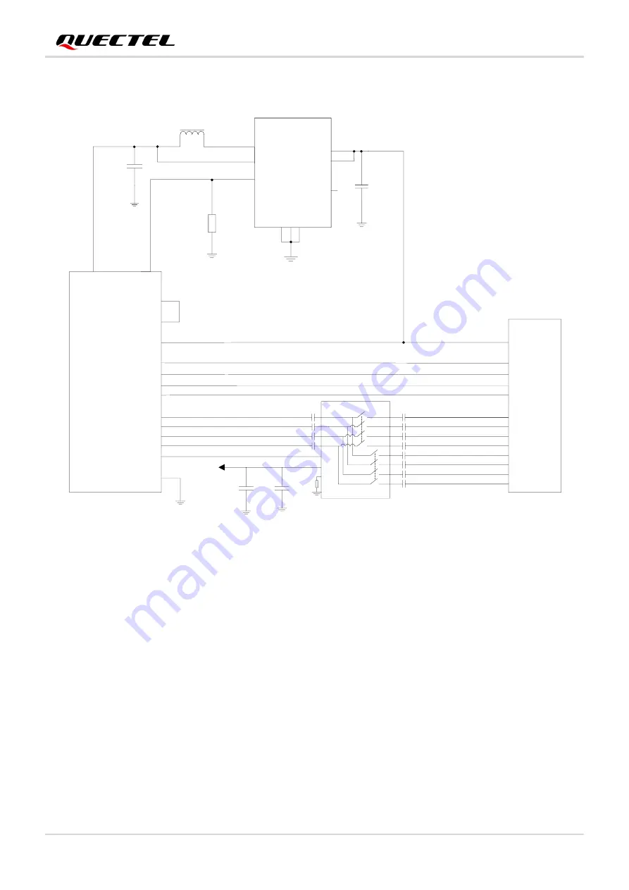
The following is a reference design for the USB Type-C interface:
USB_DP
100 nF
Module
C14
Switch
C2
C3
C4
C5
A0+
A0-
A1+
A0-
B0+
B0-
B1+
B1-
C0+
C0-
C1+
C1-
SEL
PD
USB_SS_TX_P
USB_SS_TX_M
USB_SS_RX_P
USB_SS_RX_M
USB_SS_ SEL
R1
VDD
4.7
μ
F
C1
VDD_3V0
TX1+
TX1-
VBUS_ VBUS
CC1
D+
D-
RX1-
RX1+
CC2
CC1
CC2
TX2+
TX2-
RX2+
RX2-
USB Type_C
C6
C7
C8
C9
C10
C11
C12
C13
USB_DM
USB_ VBUS
USB_ID
GPIO_1
AW3605DNR
SW
VIN
22
μ
F
C2
10
μ
F
10K
1.0
μ
H
C1
L1
R1
EN
A
G
N
D
VOUT
VOUT
NC
P
G
N
D
P
G
N
D
1
2
9
4
5
6
7
8
VBUS
VPH_PWR GPIO_97
3
Figure 12: USB Type-C Interface Reference Design
To ensure sound USB performance, please follow these principles in your design:
⚫
Route the USB signal traces as differential pairs with total grounding and keep the impedance of USB
differential traces at 90
Ω.
⚫
Pay attention to the influence of junction capacitance of ESD protection devices upon USB data lines.
Typically, the capacitance should be less than 2 pF for USB 2.0 and less than 0.5 pF for USB 3.0.
⚫
Avoid routing the USB signal traces under crystals, oscillators, magnetic devices, or RF signal traces.
Route the traces in the inner-layer of PCB with ground shielding on not only upper and lower layers
but also right and left sides.
⚫
Keep the ESD protection devices as close to the USB connector as possible.
⚫
Ensure the trace length differences between the USB 2.0 DM/DP differential pair and between the
USB 3.0 RX/TX differential pairs do not exceed 0.7 mm.


