GNSS Module Series
LC29D_EVB(0)_User_Guide 14 / 42
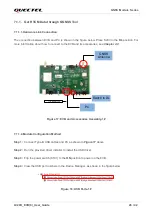
Test points distribution is shown below:
J302 pin assignment:
VDD_EXT
CTS1
RTS1
TXD1
RXD1
I2C_SDA
I2C_SCL
1PPS
GND
VCC_3.3V
Table 3: J302 Pin Detailed Description
J501 pin assignment:
NC
NC
NC
NC
NC
WHEELTICK
FWD
GND
J202
SD Card Connector
The data received by the SD card and
Standard COM Port
are the same.
Test Points
J302
Test Points
Pins are detailed in
Table 3
below.
J501
ODO Connector
Pins are detailed in
Table 4
below.
Pin Name
I/O
Description
VDD_EXT
-
Reserved
CTS1
DO
Clear to send
RTS1
DO
Request to send
TXD1
DO
Transmits data
RXD1
DI
Receives data
I2C_SDA
-
Reserved
I2C_SCL
-
Reserved
1PPS
DO
1 pulse per second
GND
-
Ground
VCC_3.3V
PO
3.3 V power output


