PDP-436SXE
79
5
6
7
8
5
6
7
8
C
D
F
A
B
E
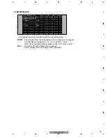
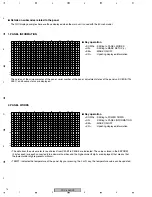
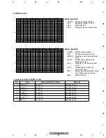
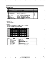
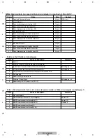
8. ETC.
<Lower-layer items of ETC.>
• "NO OPRT" is selected when this submode is entered (to avoid accidental misoperation).
• When each item is set, the process starts then the unit shifts to the upper layer. (When NO OPRT is determined,
the unit will shift to the upper layer without doing anything.)
• When BACK UP DATA are set to be backed up, if the digital EEPROM has not been adjusted,
LED operation becomes that RED LED BLUE LED flashes (200ms).
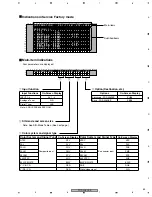
A
.
P
N E L
L
/
1
[
B
T
6 0 V S ]
I
–
N 1
5
2
0 6 0
– R G B
H
E
–
S 6
F A C T
T
E
C .
)
( +
1
5
10
15
16
1
5
10
15
20
25
30
32
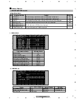
A
.
P
N E L
L
/
1
[
B
T
6 0 V S ]
I
–
N 1
5
2
0 6 0
– R G B
H
E
–
S 6
F A C T
A
P R O M
B
C K U P
E E
>
< =
T
E
C .
O
: N
P R T
O
1
5
10
15
16
1
5
10
15
20
25
30
32
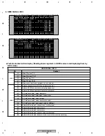
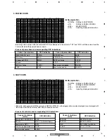
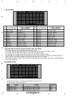
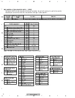
<DOWN> : Shifting to MASK SETUP (+)
<UP>
: Shifting to PANEL REVISE (+)
<SEL>
: MASK ON/OFF
<SET>
: Shifting to the next nested layer
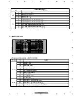
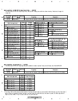
7
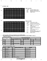
Key operation
<DOWN> : Shifting to the next item
<UP>
: Shifting to the previous item
<RIGHT> : Adding by one to the adjustment
value
<LEFT>
: Subtracting by one from the
adjustment value
<SET>
: Determining the setting value
and shifting to the upper layer
<SEL>
: MASK ON/OFF
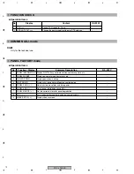
7
Key operation
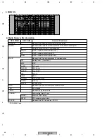
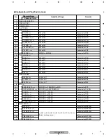
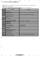
No.
Items
Adjustment/Setting Value
Remarks
1
BACKUP DATA <=>
<=>NO OPRT<=>TRANSFER<=>
"ERR" is indicated when no data are in the backup
EEPROM. To activate the option to select
TRANSFER, press the SET key about 5 seconds.
(There is a situation resting more than 5 seconds.)
2
DIGITAL EEPROM <=> <=>NO OPRT<=>REPAIR/DELETE<=>
"DELETE" is indicated when the panel unit has been
already adjusted. To activate the option to select
REPAIR/DELETE, press the SET key about 5
seconds.
(There is a situation resting more than 5 seconds.)
3
PD INFO. <=>
<=>NO OPRT<=>CLEAR<=>
To activate the option to select CLEAR, repeatedly
press the SET key about 5 seconds.
(There is a situation resting more than 5 seconds.)
4
SD INFO. <=>
<=>NO OPRT<=>CLEAR<=>
5
HR-MTR INFO. <=>
<=>NO OPRT<=>CLEAR<=>
6
PM/B1-B5 <=>
<=>NO OPRT<=>CLEAR<=>
7
P-COUNT INFO. <=>
<=>NO OPRT<=>CLEAR<=>
Содержание PDP-436RXE
Страница 9: ...PDP 436SXE 9 5 6 7 8 5 6 7 8 C D F A B E ...
Страница 25: ...PDP 436SXE 25 5 6 7 8 5 6 7 8 C D F A B E SXE Only SXE Only ...
Страница 27: ...PDP 436SXE 27 5 6 7 8 5 6 7 8 C D F A B E SXE Only SXE Only SXE Only ...
Страница 145: ...PDP 436SXE 145 5 6 7 8 5 6 7 8 C D F A B E Block Diagram R2S11002AFT OBE MAIN ASSY IC4804 AV SW ...
Страница 146: ...PDP 436SXE 146 1 2 3 4 1 2 3 4 C D F A B E Block Diagram R2S11001FT OBE MAIN ASSY IC4806 Component SW IC ...

