background image

1997 Feb 27

21

Philips Semiconductors

Product specification

IF amplifier/demodulator for FM radio receivers

TDA1597

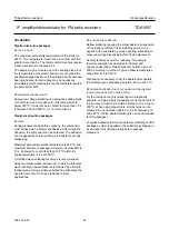
SOLDERING

Plastic dual in-line packages

B

Y DIP OR WAVE

The maximum permissible temperature of the solder is
260

°

C; this temperature must not be in contact with the

joint for more than 5 s. The total contact time of successive
solder waves must not exceed 5 s.

The device may be mounted up to the seating plane, but
the temperature of the plastic body must not exceed the
specified storage maximum. If the printed-circuit board has
been pre-heated, forced cooling may be necessary
immediately after soldering to keep the temperature within
the permissible limit.

R

EPAIRING SOLDERED JOINTS

Apply a low voltage soldering iron below the seating plane
(or not more than 2 mm above it). If its temperature is
below 300

°

C, it must not be in contact for more than 10 s;

if between 300 and 400

°

C, for not more than 5 s.

Plastic small outline packages

B

Y WAVE

During placement and before soldering, the component
must be fixed with a droplet of adhesive. After curing the
adhesive, the component can be soldered. The adhesive
can be applied by screen printing, pin transfer or syringe
dispensing.

Maximum permissible solder temperature is 260

°

C, and

maximum duration of package immersion in solder bath is
10 s, if allowed to cool to less than 150

°

C within 6 s.

Typical dwell time is 4 s at 250

°

C.

A modified wave soldering technique is recommended
using two solder waves (dual-wave), in which a turbulent
wave with high upward pressure is followed by a smooth
laminar wave. Using a mildly-activated flux eliminates the
need for removal of corrosive residues in most
applications.

B

Y SOLDER PASTE REFLOW

Reflow soldering requires the solder paste (a suspension
of fine solder particles, flux and binding agent) to be
applied to the substrate by screen printing, stencilling or
pressure-syringe dispensing before device placement.

Several techniques exist for reflowing; for example,
thermal conduction by heated belt, infrared, and
vapour-phase reflow. Dwell times vary between 50 and
300 s according to method. Typical reflow temperatures
range from 215 to 250

°

C.

Preheating is necessary to dry the paste and evaporate
the binding agent. Preheating duration: 45 min at 45

°

C.

R

EPAIRING SOLDERED JOINTS

(

BY HAND

-

HELD SOLDERING

IRON OR PULSE

-

HEATED SOLDER TOOL

)

Fix the component by first soldering two, diagonally
opposite, end pins. Apply the heating tool to the flat part of
the pin only. Contact time must be limited to 10 s at up to
300

°

C. When using proper tools, all other pins can be

soldered in one operation within 2 to 5 s at between 270
and 320

°

C. (Pulse-heated soldering is not recommended

for SO packages.)

For pulse-heated solder tool (resistance) soldering of VSO
packages, solder is applied to the substrate by dipping or
by an extra thick tin/lead plating before package
placement.

Содержание TDA1597

Страница 1: ...DATA SHEET Product specification Supersedes data of May 1994 File under Integrated Circuits IC01 1997 Feb 27 INTEGRATED CIRCUITS TDA1597 IF amplifier demodulator for FM radio receivers ...

Страница 2: ... home and car FM radio receivers and is suitable for mono and stereo reception It may also be applied to common front ends stereo decoders and AM receivers circuits All pin numbers mentioned in this data sheet refer to the SO version TDA1597T unless otherwise specified QUICK REFERENCE DATA ORDERING INFORMATION SYMBOL PARAMETER CONDITIONS MIN TYP MAX UNIT VP supply voltage 7 5 8 5 12 V IP supply cu...

Страница 3: ... int V ref V ref V P 8 5 V V offset V int V int V ref V int 5 V V ref V ref V oAF 25 kΩ 25 kΩ 40 kΩ 40 kΩ 3 3 kΩ 7 5 kΩ 25 kΩ 330 Ω V int 9 pF 22 nF 22 nF 19 17 18 16 17 15 13 11 16 14 15 13 14 12 1 20 18 SFE FM IF input 9 pF 1 1 2 2 3 3 4 4 2 3 4 MPX signal weighted level information FM OFF MUTE OFF 5 5 6 6 100 nF 7 7 8 8 9 47 nF 100 pF 25 kΩ 25 kΩ STOP 0 STOP 1 n c Q L 19 MED829 12 11 10 10 9 n ...

Страница 4: ...I2 10 11 demodulator input 2 n c 12 not connected TSW 11 13 tau switch input ST1 12 14 STOP 1 stop pulse output 1 ST0 13 15 STOP 0 stop pulse output 0 MUTE 14 16 muting voltage GND 15 17 ground 0 V LFB1 16 18 IF limiter feedback 1 LFB2 17 19 IF limiter feedback 2 ViIF 18 20 IF signal input Fig 2 Pin configuration DIP version handbook halfpage TDA1597 MED830 1 2 3 4 5 6 7 8 9 18 17 16 15 14 13 12 1...

Страница 5: ...e control voltage for the mute attenuator pin 16 is derived from the values of the level detector and the detuning detector output signals The mute attenuator has a fast attack and a slow decay determined by the capacitor connected to pin 16 The AF signal is fed via the mute attenuator to the output pin 4 A weighted control voltage pin 6 is obtained from the mute attenuator control voltage via a b...

Страница 6: ...E OFF 0 9Vref V FM OFF AF attenuation 60 dB 1 4 V IF amplifier and demodulator Zi demodulator input impedance between pins 10 and 11 25 40 55 kΩ Ci demodulator input capacitance between pins 10 and 11 6 pF AF output pin 4 Ro output resistance 400 Ω V4 DC output voltage level ViIF 5 µV RMS on pin 20 2 75 3 1 3 45 V PSRR power supply ripple rejection pin 4 f 1000 Hz Vripple 50 mV RMS 33 36 dB Tuning...

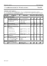
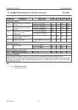
Страница 7: ...vel detector R6 output resistance pin 6 500 Ω V6 output voltage at I2 0 V20 5 µV RMS see Fig 14 0 1 1 1 V V20 1 mV RMS 3 0 4 2 V 200 kHz detuning 1 2 1 5 1 8 V output voltage at V2 V5 V20 5 µV RMS 0 3 V V6 output voltage at detuning 45 kHz detuning 0 2 V TC temperature coefficient 3 3 mV VK f detuning frequency V6 1 8 V see Fig 13 90 160 kHz S steepness of control voltage slope 50 µV V20 50 mV 1 4...

Страница 8: ...7 Vref FM MUTE OFF 14 22 35 µV input signal for signal to noise ratio RMS value f 250 to 15000 Hz V7 Vref S N 26 dB 15 µV S N 46 dB 60 µV S N signal to noise ratio deviation 75 kHz 82 dB Vo rms AF output signal RMS value pin 4 180 200 220 mV THD total harmonic distortion without de emphasis without detuning deviation 75 kHz fm 1 kHz I7 0 0 1 0 3 25 kHz detuning deviation 75 kHz fm 1 kHz I7 0 0 6 c...

Страница 9: ... of detune detector 12 25 50 kΩ V8 voltage on capacitor Vi 5 µV RMS on input pin 20 I7 0 2 2 V Level detector I2 0 V6 output voltage V20 5 µV RMS 0 1 1 1 V V20 1 mV RMS 3 0 4 2 V Reference voltage source pin 5 Vref reference output voltage I5 1 mA 3 3 3 7 4 1 V Operation with AM IF Level and stop information on pins 6 13 14 15 and 16 is provided for the modes FM MUTE ON and FM MUTE OFF This inform...

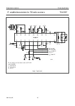
Страница 10: ...2 FM MUTE ON 3 FM OFF handbook full pagewidth MED832 1 1 2 2 3 3 20 18 4 4 5 5 6 6 7 7 S4 100 nF 1 3 2 8 8 9 10 11 10 12 5 V STOP 1 STOP 0 Vmute 13 11 14 12 15 13 16 14 17 15 9 n c n c level weighted level unweighted VoAF unweighted VoAF weighted Vref 3 7 V 10 Ω 220 kΩ 3 9 kΩ 10 kΩ S3 S2 4 7 nF 100 nF 8 5 V VP S1 3 3 kΩ 100 pF 220 nF 47 nF 22 nF IF 10 7 MHz 22 nF R1 150 Ω R2 50 Ω 27 kΩ 18 16 19 17...

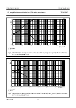
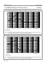
Страница 11: ...20 with f 22 5 kHz fm 1 kHz de emphasis 50 µs 1 Audio signal 2 Noise 0 10 6 10 5 10 4 10 3 10 2 10 1 1 MBE519 20 40 60 80 100 Vi20 rms V V4 dB 1 2 Fig 6 FM MUTE OFF Audio signal and noise as functions of the input signal ViIF pin 20 with f 22 5 kHz fm 1 kHz de emphasis 50 µs 1 Audio signal 2 Noise handbook full pagewidth 20 V4 dB 20 40 60 80 0 MEH071 10 6 10 5 10 4 10 3 10 2 10 1 1 1 2 Vi20 rms V ...

Страница 12: ...of the input signal ViIF pin 20 with f 22 5 kHz fm 1 kHz AM with fm 400 Hz m 0 3 and 250 to 15000 Hz bandwidth 1 Audio signal 2 Spurious AM signal Fig 8 FM MUTE OFF Typical AM suppression as a function of the input signal ViIF pin 20 with f 22 5 kHz fm 1 kHz AM with fm 400 Hz m 0 3 and 250 to 15000 Hz bandwidth 1 Audio signal 2 Spurious AM signal handbook full pagewidth 20 V4 dB 20 40 60 80 0 MEH0...

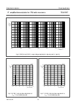
Страница 13: ...n 20 handbook full pagewidth 10 V14 15 12 13 V 0 2 4 6 8 MEH074 10 6 10 5 10 4 10 3 10 2 10 1 1 Vi20 rms V Fig 10 STOP 1 output voltage dependent on ViIF 10 mV RMS pin 20 handbook halfpage 10 0 8 6 4 2 MED833 detune kHz V14 12 V 40 30 20 10 10 20 0 Fig 11 STOP 0 output voltage dependent on ViIF 10 mV RMS pin 20 handbook halfpage 10 0 8 6 4 2 MEH075 detune kHz V15 13 V 20 10 10 20 30 40 0 ...

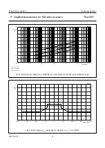
Страница 14: ...dependent on input signal ViIF pin 20 typical adjusting range 1 V2 0 V 2 I2 0 mA 3 V2 Vref handbook full pagewidth 10 V16 14 V 0 2 4 6 8 MEH076 10 6 10 5 10 4 10 3 10 2 10 1 1 1 2 3 Vi20 rms V Fig 13 Mute voltage V16 14 dependent on detuning ViIF 10 mV RMS handbook full pagewidth detune kHz 10 0 400 300 V16 14 V 200 100 100 0 200 300 400 2 4 6 8 MEH079 ...

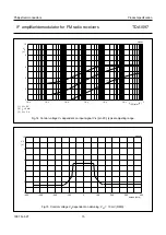
Страница 15: ...voltage V6 dependent on input signal ViIF pin 20 typical adjusting range 1 V2 0 V 2 I2 0 mA 3 V2 Vref 10 0 10 6 10 5 10 4 10 3 10 2 10 1 1 MBE516 2 4 6 8 Vi20 rms V V6 V 1 2 3 Fig 15 Control voltage V6 dependent on detuning ViIF 10 mV RMS handbook full pagewidth detune kHz 10 0 400 300 V6 V 200 100 100 0 200 300 400 2 4 6 8 MED834 ...

Страница 16: ...ndent on input signal ViIF pin 20 typical adjusting range 1 V2 0 V 2 I2 0 mA 3 V2 Vref 10 0 10 6 10 5 10 4 10 3 10 2 10 1 1 MBE517 2 4 6 8 Vi20 rms V V V3 1 2 3 Fig 17 Total harmonic distortion dependent on detuning at FM MUTE ON f 75 kHz fm 1 kHz ViIF 10 mV handbook full pagewidth 0 5 0 80 60 40 20 0 20 40 60 80 MBE518 0 1 0 2 0 3 0 4 detune kHz THD ...

Страница 17: ...g 18 Interface for AM stop pulse application SO version handbook full pagewidth MED836 1 2 3 20 4 BAW62 5 6 7 8 10 11 tuned to AM IF 12 13 14 15 16 17 9 15 kΩ 560 pF 22 nF 22 nF 22 nF SFE FM IF 300 Ω AM IF HIGH FM LOW AM tuned to FM IF 3 3 kΩ 100 pF 18 19 TDA1597T 1 2 3 20 4 5 6 7 8 10 11 12 13 14 15 16 17 9 18 19 TDA1572T STOP 1 STOP 0 1 kΩ ...

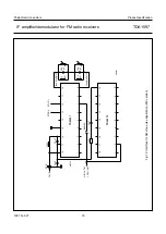
Страница 18: ...Interface for AM stop pulse application DIP version handbook full pagewidth MED837 1 2 3 18 4 BAW62 5 6 7 8 10 tuned to AM IF 11 12 13 14 15 9 15 kΩ 560 pF 22 nF 22 nF 22 nF SFE FM IF 300 Ω AM IF HIGH FM LOW AM tuned to FM IF 3 3 kΩ 100 pF 16 17 TDA1597 1 2 3 18 4 5 6 7 8 10 11 12 13 14 15 9 16 17 TDA1572 STOP 1 STOP 0 1 kΩ ...

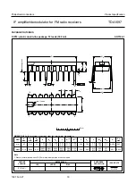
Страница 19: ...mm dimensions A min A max b max w ME e1 1 40 1 14 0 53 0 38 0 32 0 23 21 8 21 4 6 48 6 20 3 9 3 4 0 254 2 54 7 62 8 25 7 80 9 5 8 3 0 85 4 7 0 51 3 7 inches 0 055 0 044 0 021 0 015 0 013 0 009 1 40 1 14 0 055 0 044 0 86 0 84 0 26 0 24 0 15 0 13 0 01 0 10 0 30 0 32 0 31 0 37 0 33 0 033 0 19 0 020 0 15 MH c e 1 ME A L seating plane A1 w M b1 b2 e D A2 Z 18 1 10 9 b E pin 1 index 0 5 10 mm scale Note...

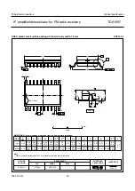
Страница 20: ...0 o o 0 25 0 1 DIMENSIONS inch dimensions are derived from the original mm dimensions Note 1 Plastic or metal protrusions of 0 15 mm maximum per side are not included 1 1 0 4 SOT163 1 92 11 17 95 01 24 10 20 w M bp detail X Z e 11 1 D y 0 25 075E04 MS 013AC pin 1 index 0 10 0 012 0 004 0 096 0 089 0 019 0 014 0 013 0 009 0 51 0 49 0 30 0 29 0 050 1 4 0 055 0 42 0 39 0 043 0 039 0 035 0 016 0 01 0 ...

Страница 21: ...s than 150 C within 6 s Typical dwell time is 4 s at 250 C A modified wave soldering technique is recommended using two solder waves dual wave in which a turbulent wave with high upward pressure is followed by a smooth laminar wave Using a mildly activated flux eliminates the need for removal of corrosive residues in most applications BY SOLDER PASTE REFLOW Reflow soldering requires the solder pas...

Страница 22: ...r goal specifications for product development Preliminary specification This data sheet contains preliminary data supplementary data may be published later Product specification This data sheet contains final product specifications Limiting values Limiting values given are in accordance with the Absolute Maximum Rating System IEC 134 Stress above one or more of the limiting values may cause perman...

Страница 23: ...1997 Feb 27 23 Philips Semiconductors Product specification IF amplifier demodulator for FM radio receivers TDA1597 NOTES ...

Страница 24: ...EX UB3 5BX Tel 44 181 730 5000 Fax 44 181 754 8421 United States 811 East Arques Avenue SUNNYVALE CA 94088 3409 Tel 1 800 234 7381 Uruguay see South America Vietnam see Singapore Yugoslavia PHILIPS Trg N Pasica 5 v 11000 BEOGRAD Tel 381 11 625 344 Fax 381 11 635 777 For all other countries apply to Philips Semiconductors Marketing Sales Communications Building BE p P O Box 218 5600 MD EINDHOVEN Th...

Отзывы: