Circuit descriptions and abbreviation list
GB 91
EM1A
9.
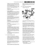
flowing in L5422 (1-2). The voltage across the deflection coil
increases, so the picture width increases. When TS7480
blocks, C2421 will not discharge anymore and the voltage
across C2421 will remain constant. The result is that the
voltage across the deflection coil is minimal. The voltage
across coil L5422, however, is maximal. This coil (L5422)
consists of a transformer:
•
As the current through the coil 1-2 increases (smaller
picture width), the current through coil 3-4 decreases.
Because of the transformer characteristic a higher
voltage will be subjected to coil 3-4, which will counteract
the current. The current will diminish even further.
•
When the current through coil 1-2 diminishes (larger
picture width), the current through coil 3-4 increases.
The EW Drive
The EW drive signal originates in the HOP and is supplied to
TS7480. The shape of this signal determines the various
geometric correction parameters:
•
H amplitude
•
EW-parabola
•
EW-corner
•
EW-trapezium
•
Horizontal parallelogram
•
Horizontal bow
Beam current correction
The EHT-info at point 10 of the LOT is dependent on the
value of the beam current and the voltage divider R3450,
R3451 and C2450. The EHT-info is fed to the HOP to trim the
contrast and to compensate for the changes in picture-width
as a function of the EHT-info, when the high-voltage is
decreased. The EHT-info is integrated via C2450 and sent
to the gate of the E/W FET (TS7480) as a DC-voltage to
correct the EW-current.
9.1.11 Vertical (frame) deflection (diagram A4)
Driving the frame output stage
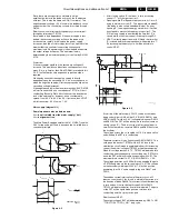
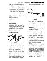
Figure 9-11
The HOP drives the frame output stage. As the HOP is 'cold'
and the frame output stage is 'hot', they must be galvanic
isolated. This is done by means of an optocoupler. In the MG-
chassis the HOP generates 3 signals needed for the frame
output stage: VDPOS, VDNEG and FRAME ROTATION. To
avoid the costs of 3 optocouplers, the frame drive pulse and
rotation DC-voltage are added together and then fed to
optocoupler TS7610.This is done as follows:
The VD100 signal from the PICNIC (diagram B3 pin 19) is
extended for 16.5 lines and inverted via a monostable
multivibrator (TS7311 & TS7309, diagram B4). The output
signal VDHOP is then superimposed on a DC-voltage from
pin 25 of the HOP. The resulting signal is called
FRA and is fed to optocoupler 7610 (diagram
A4). So this signal contains info for both the frame deflection
and the frame rotation (if present).
The circuit around IC7440 will amplify this signal and the
output current will flow through the rotation coil. The vertical
pulses on this signal are filtered by C2445 to ensure that only
a DC-voltage will be supplied to the rotation coil.
The output voltage of the rotation circuit is between -8 and +8
V.
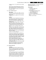
Figure 9-12
The sawtooth voltage for the frame output stage is not
generated by the HOP but by a discrete circuit after the
optocoupler 7610: via R3600 and R3601 a linear increasing
voltage over C2601 is built up with a large time constant.
The circuit around TS7603 is a current source, driving C2601
with a current value derived from the E/W modulator. This will
result in an S-shaped voltage on C2601 (also known as EW-
correction).
Flyback generator
The frame output stage is supplied via the +13 V and -15 V
coming from the LOT. The output of the amplifier is 0 VDC,
so a coupling capacitor is not required.
During the (forward) scan, a supply of +13 and -15 V is
sufficient to respond to the slow changing current. The
flyback generator puts a voltage of -15 V on pin 3. Because
of the voltage drop over zenerdiode D6622 (8.2 V), C2622
will be charged to 19 V: being 13 + (15 - 8.2 - 0.7) V.
During the flyback scan, the change in current per time is
much larger, so a higher voltage is required. The flyback
generator will now generate a voltage of +13 V on pin 3.
Added to the charge on C2622 this will give a flyback voltage
of 32 V (depending on the CRT size, this value can differ).
The IC amplifier (IC7620, pin 5) supplies the sawtooth
current to the frame deflection coil. The current through this
coil is measured via R3620//R3621//R3622 and fed back to
the inverting input of the amplifier.
R3624 and C2624 on the output of the amplifier, form a filter
for high frequencies and in that way also prevents
oscillations.
Peak voltages on the output, e.g. as a result of a possible
flash, are damped by the clamp circuit consisting of D6619,
C2627 and R3627. The network consisting of R3625, R3629
and C2629 form an extra damping circuit.
Protection circuit for bridge-coil and frame output stage
The secondary voltage of bridge coil L5422 is guarded at the
diode modulator (D6421/22) via a detection circuit consisting
of an 8.2 V zenerdiode (diagram A3). When the bridge-coil is
working properly, the average voltage on D6422 is such that
this zenerdiode will conduct and will drive TS7652 into
saturation via the BRIDGE_PROT signal (see diagram A4).
When, for any reason, the secondary side of the bridge-coil
is shorted, the average voltage on D6422 will drop below the
zener-voltage and TS7652 will block. Now capacitor C2642
will be charged. Transistor TS7407 will start conducting and
the STANDBY signal will be grounded via R3403. This will
switch off the main supply (see diagram A1).
2601
470n
6600
HOT
COLD
FRA
+13V_LOT
+13V_LOT
141V
V
DHOP
(6-BITS DAC) 25
HOP
3388
3630
3619
3632
3440
ROTATION
CIRCUIT
3631
7605
3390
3394
3386
3391
7312
7310
3389
+8V
CL 96532156_026.eps
210100
7606
3601
2M2
3600
2M2
A
7610
V
SYNC
2601
2602
+13V
+13V
+12V
3615
141V
3606
3612
3614
7600
7603
2600
CL 96532156_027.eps
070100
3602
3618
3603
3601
3633
3600
-15V
3605
3609
3610
3620//21//22
3623
7602
3607
3608
7620
V. AMPL.
V. SHIFT
E/W
-
+
1
7
5
V
OUT
I
COIL
FRAME
DEFL.
COIL
A


