Page 133
T
5CL8
CLR (TC6CR).3: Stops the timer.
CLR (TC6CR).7 : Sets the
PWM
6 pin to the high level.
Note 3: To enter the STOP mode, stop the timer and then enter the STOP mode. If the STOP mode is entered with-
out stopping of the timer when fc, fc/2 or fs is selected as the source clock, a pulse is output from the
PWM
6
pin during the warm-up period time after exiting the STOP mode.
Table 11-7 16-Bit PWM Output Mode
Source Clock
Resolution
Repeated Cycle
NORMAL1/2, IDLE1/2 mode
SLOW1/2,
SLEEP1/2
mode
fc = 16 MHz
fs = 32.768 kHz
fc = 16 MHz
fs = 32.768 kHz
DV7CK = 0
DV7CK = 1
fc/2
11
fs/2
3
[Hz]
fs/2
3
[Hz]
128
µ
s
244.14
µ
s
8.39 s
16 s
fc/2
7
fc/2
7
–
8
µ
s
–
524.3 ms
–
fc/2
5
fc/2
5
–
2
µ
s
–
131.1 ms
–
fc/2
3
fc/2
3
–
500 ns
–
32.8 ms
–
fs
fs
fs
30.5
µ
s
30.5
µ
s
2 s
2 s
fc/2
fc/2
–
125 ns
–
8.2 ms
–
fc
fc
–
62.5 ns
–
4.1 ms
–
Example :Generating a pulse with 1-ms high-level width and a period of 32.768 ms (fc = 16.0 MHz)
Setting ports
LDW
(PWREG5), 07D0H
: Sets the pulse width.
LD
(TC5CR), 33H
: Sets the operating clock to fc/2
3
, and 16-bit PWM output
mode (lower byte).
LD
(TC6CR), 056H
: Sets TFF6 to the initial value 0, and 16-bit PWM signal
generation mode (upper byte).
LD
(TC6CR), 05EH
: Starts the timer.
Содержание CEM2100/00
Страница 2: ...2 ...
Страница 3: ...BLOCK DIAGRAM ...
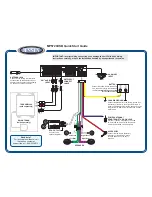
Страница 4: ...WIRING DIAGRAM 4 ...
Страница 5: ...CIRCUIT DIAGRAM MAIN BOARD 5 ...
Страница 6: ...6 ...
Страница 7: ......
Страница 11: ...PCB LAYOUT MAIN BOARD TOP SIDE VIEW 11 ...
Страница 12: ...PCB LAYOUT MAIN BOARD BOTTOM SIDE VIEW 12 ...
Страница 13: ...PCB LAYOUT PANEL BOARD TOP SIDE VIEW ...
Страница 14: ...14 PCB LAYOUT PANEL BOARD BOTTOM SIDE VIEW ...
Страница 15: ...PCB LAYOUT REMOTE BOARD TOP SIDE VIEW 15 ...
Страница 16: ...PCB LAYOUT REMOTE BOARD BOTTOM SIDE VIEW 16 ...
Страница 17: ...PCB LAYOUT TUNER BOARD TOP SIDE VIEW 17 ...
Страница 18: ...PCB LAYOUT TUNER BOARD BOTTOM SIDE VIEW 18 ...
Страница 19: ...PCB LAYOUT SD BOARD TOP SIDE VIEW ...
Страница 20: ...20 PCB LAYOUT CD CONNECTOR TOP SIDE VIEW ...
Страница 21: ...PCB LAYOUT ISO BOARD BOTTOM SIDE VIEW 21 ...
Страница 22: ...22 SET EXPLODER VIEW DRAWING ...
Страница 23: ...1 of 2 CEM2100 Trouble shooting Trouble shooting Trouble shooting Trouble shooting ...
Страница 33: ...7 0 6SHFLILFDWLRQ 6 VWHP EORFN GLDJUDP ...
Страница 110: ...7 0 6SHFLILFDWLRQ 5HYLVLRQ KLVWRU 2 2 s u 2 u 2 7 t 2 2 2 S S 5 2 v 2 2 ...
Страница 111: ...8 Bit Microcontroller TLCS 870 C Series T5CL8 ...
Страница 113: ...Revision History Date Revision 2008 7 31 1 First Release ...
Страница 114: ......
Страница 122: ...viii ...
Страница 126: ...Page 4 1 3 Block Diagram T5CL8 1 3 Block Diagram Figure 1 2 Block Diagram ...
Страница 130: ...Page 8 1 4 Pin Names and Functions T5CL8 ...
Страница 155: ...Page 33 T5CL8 ...
Страница 156: ...Page 34 2 Operational Description 2 3 Reset Circuit T5CL8 ...
Страница 186: ...Page 64 5 I O Ports 5 8 Port P7 P77 to P70 T5CL8 ...
Страница 194: ...Page 72 6 Watchdog Timer WDT 6 3 Address Trap T5CL8 ...
Страница 214: ...Page 92 8 16 Bit TimerCounter 1 TC1 8 3 Function T5CL8 ...
Страница 270: ...Page 148 12 Asynchronous Serial interface UART1 12 9 Status Flag T5CL8 ...
Страница 280: ...Page 158 13 Asynchronous Serial interface UART2 13 9 Status Flag T5CL8 ...
Страница 332: ...Page 210 16 Serial Bus Interface I2C Bus Ver D SBI 16 6 Data Transfer of I2C Bus T5CL8 ...
Страница 342: ...Page 220 17 10 bit AD Converter ADC 17 6 Precautions about AD Converter T5CL8 ...
Страница 354: ...Page 232 19 Flash Memory 19 4 Access to the Flash Memory Area T5CL8 ...
Страница 388: ...Page 266 21 Input Output Circuit 21 2 Input Output Ports T5CL8 ...
Страница 397: ...Page 275 T5CL8 23 Package Dimensions LQFP64 P 1010 0 50D Rev 01 Unit mm ...
Страница 398: ...Page 276 23 Package Dimensions T5CL8 ...
Страница 400: ......
Страница 403: ...TC94B14MFG 2010 01 12 3 Pin Layout and Block Diagram Top View Pin Layout Top View TC94B14MFG Top View TEST1 ...
Страница 428: ...TC94B14MFG 2010 01 12 28 Package LQFP80 P 1212 0 50F Weight 0 6 g Typical ...