


Page 39
T
5CL8
3.3 Interrupt Sequence
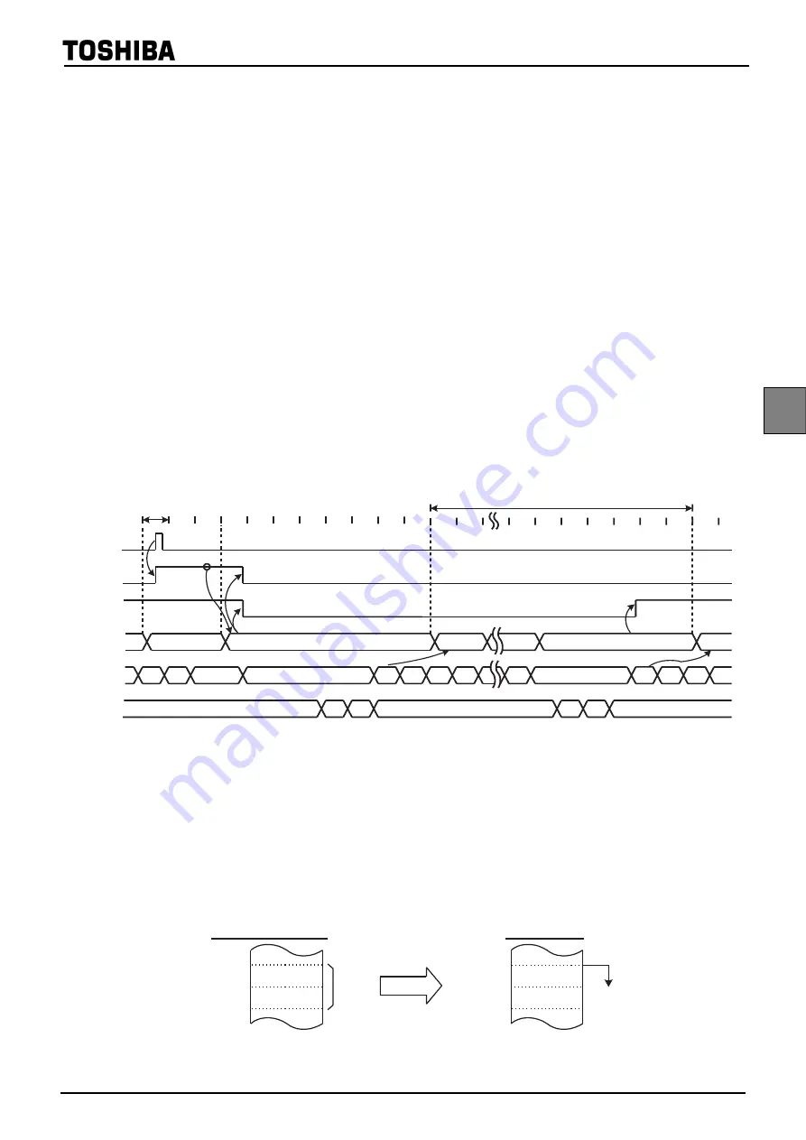
An interrupt request, which raised interrupt latch, is held, until interrupt is accepted or interrupt latch is cleared to
“0” by resetting or an instruction. Interrupt acceptance sequence requires 8 machine cycles (2
µ
s @16 MHz) after the
completion of the current instruction. The interrupt service task terminates upon execution of an interrupt return
instruction [RETI] (for maskable interrupts) or [RETN] (for non-maskable interrupts). Figure 3-1 shows the timing
chart of interrupt acceptance processing.
3.3.1 Interrupt acceptance processing is packaged as follows.
a. The interrupt master enable flag (IMF) is cleared to “0” in order to disable the acceptance of any fol-
lowing interrupt.
b. The interrupt latch (IL) for the interrupt source accepted is cleared to “0”.
c. The contents of the program counter (PC) and the program status word, including the interrupt master
enable flag (IMF), are saved (Pushed) on the stack in sequence of PSW + IMF, PCH, PCL. Mean-
while, the stack pointer (SP) is decremented by 3.
d. The entry address (Interrupt vector) of the corresponding interrupt service program, loaded on the vec-
tor table, is transferred to the program counter.
e. The instruction stored at the entry address of the interrupt service program is executed.
Note:When the contents of PSW are saved on the stack, the contents of IMF are also saved.
Note 1: a: Return address entry address, b: Entry address, c: Address which RETI instruction is stored
Note 2: On condition that interrupt is enabled, it takes 38/fc [s] or 38/fs [s] at maximum (If the interrupt latch is set at the first
machine cycle on 10 cycle instruction) to start interrupt acceptance processing since its interrupt latch is set.
Figure 3-1 Timing Chart of Interrupt Acceptance/Return Interrupt Instruction
Example: Correspondence between vector table address for INTTBT and the entry address of the interrupt
service program
Figure 3-2 Vector table address,Entry address
a
b
a
c
+
1
Execute
instruction
SP
PC
Execute
instruction
n
n
−
2
n - 3
n
−
2 n
−
1
n
−
1
n
a
+
2
a
+
1
c
+
2
b + 3
b
+
2
b
+
1
a
+
1
a
a
−
1
Execute RETI instruction
Interrupt acceptance
Execute
instruction
Interrupt service task
1-machine cycle
Interrupt
request
Interrupt
latch (IL)
IMF
D2H
03H
D203H
D204H
06H
Vector table address
Entry address
0FH
Vector
Interrupt
service
program
FFF0H
FFF1H
Содержание CEM2100/00
Страница 2: ...2 ...
Страница 3: ...BLOCK DIAGRAM ...
Страница 4: ...WIRING DIAGRAM 4 ...
Страница 5: ...CIRCUIT DIAGRAM MAIN BOARD 5 ...
Страница 6: ...6 ...
Страница 7: ......
Страница 11: ...PCB LAYOUT MAIN BOARD TOP SIDE VIEW 11 ...
Страница 12: ...PCB LAYOUT MAIN BOARD BOTTOM SIDE VIEW 12 ...
Страница 13: ...PCB LAYOUT PANEL BOARD TOP SIDE VIEW ...
Страница 14: ...14 PCB LAYOUT PANEL BOARD BOTTOM SIDE VIEW ...
Страница 15: ...PCB LAYOUT REMOTE BOARD TOP SIDE VIEW 15 ...
Страница 16: ...PCB LAYOUT REMOTE BOARD BOTTOM SIDE VIEW 16 ...
Страница 17: ...PCB LAYOUT TUNER BOARD TOP SIDE VIEW 17 ...
Страница 18: ...PCB LAYOUT TUNER BOARD BOTTOM SIDE VIEW 18 ...
Страница 19: ...PCB LAYOUT SD BOARD TOP SIDE VIEW ...
Страница 20: ...20 PCB LAYOUT CD CONNECTOR TOP SIDE VIEW ...
Страница 21: ...PCB LAYOUT ISO BOARD BOTTOM SIDE VIEW 21 ...
Страница 22: ...22 SET EXPLODER VIEW DRAWING ...
Страница 23: ...1 of 2 CEM2100 Trouble shooting Trouble shooting Trouble shooting Trouble shooting ...
Страница 33: ...7 0 6SHFLILFDWLRQ 6 VWHP EORFN GLDJUDP ...
Страница 110: ...7 0 6SHFLILFDWLRQ 5HYLVLRQ KLVWRU 2 2 s u 2 u 2 7 t 2 2 2 S S 5 2 v 2 2 ...
Страница 111: ...8 Bit Microcontroller TLCS 870 C Series T5CL8 ...
Страница 113: ...Revision History Date Revision 2008 7 31 1 First Release ...
Страница 114: ......
Страница 122: ...viii ...
Страница 126: ...Page 4 1 3 Block Diagram T5CL8 1 3 Block Diagram Figure 1 2 Block Diagram ...
Страница 130: ...Page 8 1 4 Pin Names and Functions T5CL8 ...
Страница 155: ...Page 33 T5CL8 ...
Страница 156: ...Page 34 2 Operational Description 2 3 Reset Circuit T5CL8 ...
Страница 186: ...Page 64 5 I O Ports 5 8 Port P7 P77 to P70 T5CL8 ...
Страница 194: ...Page 72 6 Watchdog Timer WDT 6 3 Address Trap T5CL8 ...
Страница 214: ...Page 92 8 16 Bit TimerCounter 1 TC1 8 3 Function T5CL8 ...
Страница 270: ...Page 148 12 Asynchronous Serial interface UART1 12 9 Status Flag T5CL8 ...
Страница 280: ...Page 158 13 Asynchronous Serial interface UART2 13 9 Status Flag T5CL8 ...
Страница 332: ...Page 210 16 Serial Bus Interface I2C Bus Ver D SBI 16 6 Data Transfer of I2C Bus T5CL8 ...
Страница 342: ...Page 220 17 10 bit AD Converter ADC 17 6 Precautions about AD Converter T5CL8 ...
Страница 354: ...Page 232 19 Flash Memory 19 4 Access to the Flash Memory Area T5CL8 ...
Страница 388: ...Page 266 21 Input Output Circuit 21 2 Input Output Ports T5CL8 ...
Страница 397: ...Page 275 T5CL8 23 Package Dimensions LQFP64 P 1010 0 50D Rev 01 Unit mm ...
Страница 398: ...Page 276 23 Package Dimensions T5CL8 ...
Страница 400: ......
Страница 403: ...TC94B14MFG 2010 01 12 3 Pin Layout and Block Diagram Top View Pin Layout Top View TC94B14MFG Top View TEST1 ...
Страница 428: ...TC94B14MFG 2010 01 12 28 Package LQFP80 P 1212 0 50F Weight 0 6 g Typical ...


