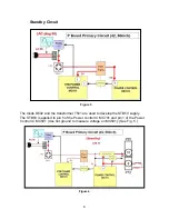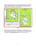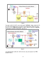
The high command at pin 17 of connector P25 is applied to pin 18 of MC701 of the P
board. Pin 11 switches from 5V to 1.3V, and pin 12 from 15V to 0V.
The 1.3V at pin 11 causes Q551 to turn on and output 5V. The 5V is applied to pin 22 of
the “Drive Voltage Oscillator” MC303. It is also applied to the “Fan SOS” circuit of the
PB board via pin 4 of the connector P30. (See Fig 14.)
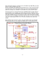
The 5V on pin 22 of IC MC303 causes it to operate. IC MC303 then turns on the Vsus
power supply circuit (MC301) and the Vda power supply circuit (IC301, and T301).
Vsus is output to SC and SS-boards. Vda is output to the Data Drive Circuit boards via
the SC board.
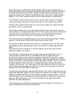
The low from pin 12 is used to turn on Q453, and Q451.
When Q453 is on, it outputs 12V to the PB board and the D board.
When Q451 is on, it outputs 15V to the PB board and the SC board
14
Содержание TH37PX50U - 37" HD PLASMA TV
Страница 40: ...SC board Waveform Figure 30 SU And SD Board Shift Registers Figure 31 35 ...
Страница 43: ...SS Board Schematic Figure 33 SS Board Waveform Figure 34 38 ...
Страница 66: ...Adjustment Volume Locations Figure 53 61 ...
Страница 67: ...Test Point Locations Figure 54 62 ...
Страница 71: ...Scan and Sustain Drive Waveform Figure 55 Scan and Sustain Drive Check points Figure 56 66 ...

